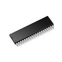
AT89C55-24PI Atmel, AT89C55-24PI Datasheet - Page 3

AT89C55-24PI
Manufacturer Part Number
AT89C55-24PI
Description
Microcontrollers (MCU) 80C31 w/20k
Manufacturer
Atmel
Datasheet
1.AT89C55-24JI.pdf
(24 pages)
Specifications of AT89C55-24PI
Data Bus Width
8 bit
Program Memory Type
Flash
Program Memory Size
20 KB
Data Ram Size
256 B
Interface Type
UART
Maximum Clock Frequency
24 MHz
Number Of Programmable I/os
32
Number Of Timers
3 x 16 bit
Operating Supply Voltage
4 V to 5.5 V
Maximum Operating Temperature
+ 85 C
Mounting Style
Through Hole
Package / Case
PDIP-40
Minimum Operating Temperature
- 40 C
Lead Free Status / Rohs Status
No
Available stocks
Company
Part Number
Manufacturer
Quantity
Price
Part Number:
AT89C55-24PI
Manufacturer:
ATMEL/爱特梅尔
Quantity:
20 000
The AT89C55 provides the following standard features:
20K bytes of Flash, 256-bytes of RAM, 32 I/O lines, three
16-bit timer/counters, a six-vector two-level interrupt archi-
tecture, a full duplex serial port, on-chip oscillator, and
clock circuitry. In addition, the AT89C55 is designed with
static logic for operation down to zero frequency and sup-
ports two software selectable power saving modes. The
Idle Mode stops the CPU while allowing the RAM,
timer/counters, serial port, and interrupt system to continue
functioning. The Power Down Mode saves the RAM con-
tents but freezes the oscillator, disabling all other chip func-
tions until the next hardware reset. The low-voltage option
saves power and operates with a 2.7-volt power supply.
Pin Description
V
Supply voltage.
GND
Ground.
Port 0
Port 0 is an 8-bit open drain bidirectional I/O port. As an
output port, each pin can sink eight TTL inputs. When 1s
are written to port 0 pins, the pins can be used as high-
impedance inputs.
Port 0 can also be configured to be the multiplexed low-
order address/data bus during accesses to external pro-
gram and data memory. In this mode, P0 has internal pul-
lups.
Port 0 also receives the code bytes during Flash program-
ming and outputs the code bytes during program verifica-
tion. External pullups are required during program verifica-
tion.
Port 1
Port 1 is an 8-bit bidirectional I/O port with internal pullups.
The Port 1 output buffers can sink/source four TTL inputs.
When 1s are written to Port 1 pins, they are pulled high by
the internal pullups and can be used as inputs. As inputs,
Port 1 pins that are externally being pulled low will source
current (I
In addition, P1.0 and P1.1 can be configured to be the
timer/counter 2 external count input (P1.0/T2) and the
timer/counter 2 trigger input (P1.1/T2EX), respectively, as
shown in the following table.
Port 1 also receives the low-order address bytes during
Flash programming and verification.
Port Pin
P1.0
P1.1
CC
IL
) because of the internal pullups.
Alternate Functions
T2 (external count input to Timer/Counter 2),
clock-out
T2EX (Timer/Counter 2 capture/reload
trigger and direction control)
Port 2
Port 2 is an 8-bit bidirectional I/O port with internal pullups.
The Port 2 output buffers can sink/source four TTL inputs.
When 1s are written to Port 2 pins, they are pulled high by
the internal pullups and can be used as inputs. As inputs,
Port 2 pins that are externally being pulled low will source
current (I
Port 2 emits the high-order address byte during fetches
from external program memory and during accesses to
external data memory that use 16-bit addresses (MOVX @
DPTR). In this application, Port 2 uses strong internal pul-
lups when emitting 1s. During accesses to external data
memory that use 8-bit addresses (MOVX @ RI), Port 2
emits the contents of the P2 Special Function Register.
Port 2 also receives the high-order address bits and some
control signals during Flash programming and verification.
Port 3
Port 3 is an 8-bit bidirectional I/O port with internal pullups.
The Port 3 output buffers can sink/source four TTL inputs.
When 1s are written to Port 3 pins, they are pulled high by
the internal pullups and can be used as inputs. As inputs,
Port 3 pins that are externally being pulled low will source
current (I
Port 3 also serves the functions of various special features
of the AT89C55, as shown in the following table.
Port 3 also receives the highest-order address bit and
some control signals for Flash programming and verifica-
tion.
RST
Reset input. A high on this pin for two machine cycles while
the oscillator is running resets the device.
Port Pin
P3.0
P3.1
P3.2
P3.3
P3.4
P3.5
P3.6
P3.7
IL
IL
) because of the internal pullups.
) because of the pullups.
Alternate Functions
RXD (serial input port)
TXD (serial output port)
INT0 (external interrupt 0)
INT1 (external interrupt 1)
T0 (timer 0 external input)
T1 (timer 1 external input)
WR (external data memory write strobe)
RD (external data memory read strobe)
4-171


