KS8721B TR Micrel Inc, KS8721B TR Datasheet
KS8721B TR
Specifications of KS8721B TR


Related parts for KS8721B TR


KS8721B TR Summary of contents
Page 1
General Description Operating at 2.5 volts to meet low voltage and low power requirements, the KS8721B/ 10BaseT/100BaseTX/FX Physical Layer Transceiver, which provides an MII to transmit and receive data. It contains the 10BaseT Physical Medium Attachment (PMA), Physical ...
Page 2
Features (continued) • LED outputs for link, activity, full/half duplex, collision and speed • Supports back to back for media converter applications • Supports MDI/MDI-X auto crossover • 2.5V/3.3V tolerance on I/O • Commercial temperature range: 0°C ...
Page 3
Revision History Revision Date Revision Date Revision Date Summary of Changes Summary of Changes Summary of Changes 1.0 1.0 1.0 1.0 2/29/02 2/29/02 2/29/02 2/29/02 Document Origination (Preliminary) Document Origination (Preliminary) Document Origination (Preliminary) Document Origination (Preliminary) 2.0 2.0 2.0 ...
Page 4
Table Of Contents Pin Description .............................................................................................................................................................6 Strapping Option ...........................................................................................................................................................9 Pin Confi guration ........................................................................................................................................................10 Introduction ............................................................................................................................................................ 11 100BaseTX Transmit ............................................................................................................................................. 11 100BaseTX Receive ............................................................................................................................................. 11 PLL Clock Synthesizer .......................................................................................................................................... PLL Clock Synthesizer .......................................................................................................................................... PLL Clock Synthesizer Scrambler/De-scrambler (100BaseTX only) ......................................................................................................... 11 ...
Page 5
Absolute Maximum Ratings .......................................................................................................................................22 Operating Ratings .......................................................................................................................................................22 Electrical Characteristics ...........................................................................................................................................22 Timing Diagrams .........................................................................................................................................................24 Selection of Isolation Transformers ..........................................................................................................................30 Selection of Reference Crystals ................................................................................................................................30 Package Outline and Dimensions .............................................................................................................................31 March 2006 5 M9999-030106 ...
Page 6
Pin Description Pin Number Pin Number Pin Number Pin Name Pin Name Pin Name Type Type Type MDIO MDIO MDIO MDIO MDIO MDC MDC MDC MDC MDC ...
Page 7
Pin Number Pin Number Pin Number Pin Name Pin Name Pin Name Type Type Type INT#/ INT#/ INT#/ INT#/ INT#/ Ipu/O Ipu/O Ipu/O Ipu/O Ipu/O PHYAD0 PHYAD0 PHYAD0 PHYAD0 PHYAD0 ...
Page 8
Pin Number Pin Number Pin Number Pin Name Pin Name Pin Name Type Type Type REXT REXT REXT REXT REXT VDDRCV VDDRCV VDDRCV VDDRCV VDDRCV ...
Page 9
Strapping Options Pin Number Pin Number Pin Number Pin Name Pin Name Pin Name Type Type Type 6,5, 6,5, 6,5, 6,5, 6,5, PHYAD[4:1]/ PHYAD[4:1]/ PHYAD[4:1]/ PHYAD[4:1]/ PHYAD[4:1]/ Ipd/O Ipd/O Ipd/O Ipd/O Ipd/O 4,3 4,3 4,3 4,3 4,3 RXD[0:3] ...
Page 10
Pin Confi guration MDIO 1 MDC 2 R3D3/PHYAD1 3 RXD2/PHYAD2 4 RXD1/PHYAD3 5 RXD0/PHYAD4 6 VDDIO 7 GND 8 RXDV/PCS_LPBK 9 RXC 10 RXER/ISO 11 GND 12 VDDC 13 TXER 14 TXC/REF_CLK 15 TXEN 16 TXD0 17 TXD1 18 TXD2 ...
Page 11
Introduction 100BaseTX Transmit The 100BaseTX transmit function performs parallel to serial conversion, NRZ to NRZI conversion, MLT-3 encoding and transmission. The circuitry starts with a parallel to serial conversion, which converts the 25MHz, 4-bit nibbles into a 125 MHz serial ...
Page 12
During auto-negotiation, the contents of Register 4, coded in Fast Link Pulse (FLP), will be sent to its link partner under the conditions of power-on, link-loss or re-start. At the same time, the KS8721B/BT will monitor incoming data to determine ...
Page 13
Collision: Whenever the line state is half-duplex and the transmitter and receiver are active at the same time, the KS8721B/ BT asserts its collision signal, which is asynchronous to any clock. RMII (Reduced MII) Data Interface RMII interface specifi es ...
Page 14
Transmit Data [1:0] (TXD[1:0]) Transmit Data TXD[1:0] shall transition synchronously with respect to REF_CLK. When TX_EN is asserted, TXD[1:0] are accepted for transmission by the PHY. TXD[1:0] shall be “00” to indicate idle when TX_EN is de-asserted. Values of TXD[1:0] ...
Page 15
RMII Receive Timing REF_CLK TXD[1:0] TXEN TXER Parameter REF_CLK Frequency RXD[1:0], CRS_DV, RX_ER Output delay from REF_CLK rising edge RXD[1:0], CRS_DV, RX_ER Output delay from REF_CLK rising edge RXD[1:0], CRS_DV, RX_ER Output delay from REF_CLK rising edge RXD[1:0], CRS_DV, RX_ER ...
Page 16
Power Management The KS8721B/BT offers the following modes for power management: • Power Down Mode: This mode can be achieved by writing to Register 0.11 or pulling pin 30 PD# Low. • Power Saving Mode: This mode can be disabled ...
Page 17
Register Map Register No. Register No. Description Description Basic Control Register Basic Control Register Basic Control Register Basic Status Register Basic Status Register Basic Status Register PHY Identifi PHY ...
Page 18
Address Address Address Address Name Name Name Name 1.10:7 1.10:7 1.10:7 1.10:7 1.10:7 1.10:7 Reserved Reserved Reserved Reserved Reserved Reserved 1.6 1.6 1.6 1.6 1.6 1.6 No Preamble No Preamble No Preamble No Preamble No Preamble No Preamble 1.5 1.5 ...
Page 19
Address Address Address Address Name Name Name Name 5.11:10 5.11:10 5.11:10 5.11:10 5.11:10 5.11:10 Pause Pause Pause Pause Pause Pause 5.9 5.9 5.9 5.9 5.9 100 BaseT4 100 BaseT4 100 BaseT4 100 BaseT4 100 BaseT4 5.8 5.8 5.8 5.8 5.8 ...
Page 20
Address Address Address Address Name Name Name Name Register 15h - RXER Counter Register 15h - RXER Counter 15.15:0 15.15:0 15.15:0 15.15:0 15.15:0 15.15:0 RXER Counter RXER Counter RXER Counter RXER Counter RXER Counter RXER Counter Register 1bh - Interrupt ...
Page 21
Address Address Address Address Name Name Name Name 1f.6 1f.6 1f.6 1f.6 1f.6 1f.6 Enable Pause Enable Pause Enable Pause Enable Pause Enable Pause Enable Pause (Flow-Control Result) (Flow-Control Result) (Flow-Control Result) 1f.5 1f.5 1f.5 1f.5 1f.5 PHY Isolate PHY ...
Page 22
Absolute Maximum Ratings Supply Voltage ( DDC DD_PLL DD_TX DD_RCV V ) ....................................................–0.5V to +3.0V DD_RX DD_RX DD_RX DD_RX DD_RX ( ......................................................–0.5V to +4.0V DDIO Input Voltage ................................................–0.5V to +4.0V Output ...
Page 23
Symbol Symbol Symbol Symbol Symbol Symbol Symbol Parameter Parameter Parameter Parameter Parameter Parameter Parameter 10BaseTX Receive R RX+/RX– Differential RX+/RX– Differential RX+/RX– Differential RX+/RX– Differential RX+/RX– Differential RX+/RX– Differential IN Input Resistance Input Resistance Input Resistance Input Resistance V Squelch ...
Page 24
Timing Diagrams TXC TXEN TXD[3:0] CRS TXP/TXM SQE Timing TXC TXEN COL Symbol Symbol Parameter Parameter t TXD [3:0] Set-Up to TXC High TXD [3:0] Set-Up to TXC High TXD [3:0] Set-Up to TXC High TXD [3:0] Set-Up to TXC ...
Page 25
TXC TXEN TXD[3:0], TXER CRS TX+/TX- Symbol Symbol Parameter Parameter t TXD [3:0] Set-Up to TXC High TXD [3:0] Set-Up to TXC High TXD [3:0] Set-Up to TXC High TXD [3:0] Set-Up to TXC High TXD [3:0] Set-Up to TXC ...
Page 26
RX+/RX- CRS RXDV RXD[3:0] RXER RXC Symbol Symbol Parameter Parameter t RXC Period RXC Period RXC Period RXC Period RXC Period RXC Period P t RXC Pulse Width RXC Pulse Width RXC Pulse Width RXC Pulse Width RXC Pulse Width ...
Page 27
TX+/TX- TX+/TX- Figure 7. Auto-Negotiation/Fast Link Pulse Timing Symbol Symbol Parameter Parameter t FLP Burst to FLP Burst FLP Burst to FLP Burst FLP Burst to FLP Burst FLP Burst to FLP Burst FLP Burst to FLP Burst FLP Burst ...
Page 28
MDC MDI O (Into Ch ip) MDI O (Out of Chip) Symbol Symbol Parameter Parameter t MDC Period MDC Period MDC Period MDC Period MDC Period MDC Period P t MDIO Set-Up to MDC (MDIO as input) MDIO Set-Up to ...
Page 29
Supply Voltage RST_N Strap-In Value Strap-In / Output Pin Symbol Symbol Parameter Parameter t Stable Supply Voltages to Reset High Stable Supply Voltages to Reset High Stable Supply Voltages to Reset High Stable Supply Voltages to Reset High Stable Supply ...
Page 30
Selection of Isolation Transformer One simple 1:1 isolation transformer is needed at the line interface. An isolation transformer with integrated common-mode choke is recommended for exceeding FCC requirements. The following table gives recommended transformer character- istics. Characteristics Name Characteristics Name ...
Page 31
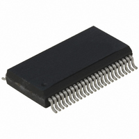
Package Information March 2006 48-Pin SSOP (SM) 31 M9999-030106 ...
Page 32
... MICREL INC. 2180 FORTUNE DRIVE SAN JOSE, CA 95131 USA + 1 (408) 944-0800 TEL This information furnished by Micrel in this data sheet is believed to be accurate and reliable. However no responsibility is assumed by Micrel for its use. Micrel reserves the right to change circuitry and specifi cations at any time without notifi cation to the customer. ...