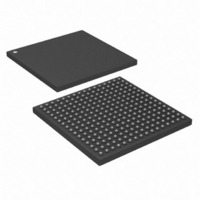
DS26514GN+ Maxim Integrated Products, DS26514GN+ Datasheet - Page 9

DS26514GN+
Manufacturer Part Number
DS26514GN+
Description
IC TXRX T1/E1/J1 4PORT 256-CSBGA
Manufacturer
Maxim Integrated Products
Type
Transceiverr
Datasheet
1.DS26514GN.pdf
(305 pages)
Specifications of DS26514GN+
Number Of Drivers/receivers
4/4
Protocol
Ethernet
Voltage - Supply
3.14 V ~ 3.47 V
Mounting Type
Surface Mount
Package / Case
256-CSBGA
Lead Free Status / RoHS Status
Lead free / RoHS Compliant
- Current page: 9 of 305
- Download datasheet (2Mb)
DS26514 4-Port T1/E1/J1 Transceiver
1.
DETAILED DESCRIPTION
The DS26514 is an 4-port monolithic device featuring independent transceivers that can be software configured for
T1, E1, or J1 operation. Each transceiver is composed of a line interface unit, framer, two HDLC controllers, elastic
store, and a TDM backplane interface. The DS26514 is controlled via an 8-bit parallel port or the SPI port. Internal
impedance matching and termination is provided for both transmit and receive paths, reducing external component
count.
Each LIU is composed of a transmit interface, receive interface, and a jitter attenuator. The transmit interface is
responsible for generating the necessary waveshapes for driving the network and providing the correct source
impedance depending on the type of media used. T1 waveform generation includes DSX-1 line build-outs as well
as CSU line build-outs of 0dB, -7.5dB, -15dB, and -22.5dB. E1 waveform generation includes G.703 waveshapes
for both 75Ω coax and 120Ω twisted cables. The receive interface provides network termination and recovers clock
and data from the network. The receive sensitivity adjusts automatically to the incoming signal level and can be
programmed for 0dB to -43dB or 0dB to -12dB for E1 applications and 0dB to -15dB or 0dB to -36dB for T1
applications. The jitter attenuator removes phase jitter from the transmitted or received signal. The crystal-less jitter
attenuator requires only a T1 or E1 clock rate, or multiple thereof, for both E1 and T1 applications, and can be
placed in either transmit or receive data paths.
On the transmit side, clock, data, and frame-sync signals are provided to the framer by the backplane interface
section. The framer inserts the appropriate synchronization framing patterns, alarm information, calculates and
inserts the CRC codes, and provides the B8ZS/HDB3 (zero code suppression) and AMI line coding. The receive-
side framer decodes AMI, B8ZS, and HDB3 line coding, synchronizes to the data stream, reports alarm
information, counts framing/coding/CRC errors, and provides clock, data, and frame-sync signals to the backplane
interface section.
There are two HDLC controllers per transceiver. Both transmit and receive paths have access to the two HDLC
controllers. One of the HDLC controllers can be assigned to some or all timeslots of the T1/E1 frame. This
controller has a FIFO depth of 256 bytes. The second controller is smaller and can be assigned to at most one
time slot, or a portion of a time slot, or to the FDL (T1) or the Sa bits (E1). This controller has a 64-byte FIFO.
The backplane interface provides a versatile method of sending and receiving data from the host system. Elastic
stores provide a method for interfacing to asynchronous systems, converting from a T1/E1 network to a 2.048MHz,
4.096MHz, 8.192MHz, 16.384MHz, or N x 64kHz system backplane. The elastic stores also manage slip conditions
(asynchronous interface). An interleave bus option (IBO) is provided to allow up to four transceivers (single
DS26514) to share a high-speed backplane. The DS26514 also contains an internal clock adapter useful for the
creation of a synchronous, high-frequency backplane timing source.
The microprocessor port provides access for configuration and status of all the DS26514’s features. Diagnostic
capabilities include loopbacks, PRBS pattern generation/detection, and 16-bit loop-up and loop-down code
generation and detection.
Rev: 101608
9 of 305
Related parts for DS26514GN+
Image
Part Number
Description
Manufacturer
Datasheet
Request
R

Part Number:
Description:
4-port T1/e1/j1 Transceiver
Manufacturer:
Maxim Integrated Products, Inc.
Datasheet:

Part Number:
Description:
power light source LUXEON® Collimator
Manufacturer:
LUMILEDS [Lumileds Lighting Company]
Datasheet:

Part Number:
Description:
MAX7528KCWPMaxim Integrated Products [CMOS Dual 8-Bit Buffered Multiplying DACs]
Manufacturer:
Maxim Integrated Products
Datasheet:

Part Number:
Description:
Single +5V, fully integrated, 1.25Gbps laser diode driver.
Manufacturer:
Maxim Integrated Products
Datasheet:

Part Number:
Description:
Single +5V, fully integrated, 155Mbps laser diode driver.
Manufacturer:
Maxim Integrated Products
Datasheet:

Part Number:
Description:
VRD11/VRD10, K8 Rev F 2/3/4-Phase PWM Controllers with Integrated Dual MOSFET Drivers
Manufacturer:
Maxim Integrated Products
Datasheet:

Part Number:
Description:
Highly Integrated Level 2 SMBus Battery Chargers
Manufacturer:
Maxim Integrated Products
Datasheet:

Part Number:
Description:
Current Monitor and Accumulator with Integrated Sense Resistor; ; Temperature Range: -40°C to +85°C
Manufacturer:
Maxim Integrated Products

Part Number:
Description:
TSSOP 14/A°/RS-485 Transceivers with Integrated 100O/120O Termination Resis
Manufacturer:
Maxim Integrated Products

Part Number:
Description:
TSSOP 14/A°/RS-485 Transceivers with Integrated 100O/120O Termination Resis
Manufacturer:
Maxim Integrated Products

Part Number:
Description:
QFN 16/A°/AC-DC and DC-DC Peak-Current-Mode Converters with Integrated Step
Manufacturer:
Maxim Integrated Products

Part Number:
Description:
TDFN/A/65V, 1A, 600KHZ, SYNCHRONOUS STEP-DOWN REGULATOR WITH INTEGRATED SWI
Manufacturer:
Maxim Integrated Products

Part Number:
Description:
Integrated Temperature Controller f
Manufacturer:
Maxim Integrated Products

Part Number:
Description:
SOT23-6/I°/45MHz to 650MHz, Integrated IF VCOs with Differential Output
Manufacturer:
Maxim Integrated Products


