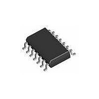
PS10NG Supertex, PS10NG Datasheet - Page 8

PS10NG
Manufacturer Part Number
PS10NG
Description
Supervisory Circuits Quad Pwr Seq Cntlr
Manufacturer
Supertex
Datasheet
1.PS10NG.pdf
(9 pages)
Specifications of PS10NG
Number Of Voltages Monitored
4
Manual Reset
Not Resettable
Watchdog
No Watchdog
Supply Voltage (max)
- 10 V
Supply Voltage (min)
- 90 V
Supply Current (typ)
450 uA
Maximum Power Dissipation
750 mW
Maximum Operating Temperature
+ 85 C
Mounting Style
SMD/SMT
Package / Case
SO-14
Minimum Operating Temperature
- 40 C
Lead Free Status / Rohs Status
Lead free / RoHS Compliant
Pin Description
Pin
10
12
13
14
11
1
2
3
4
5
6
7
8
9
PWRGD-D
PWRGD-C
PWRGD-B
PWRGD-A
Function
RAMP
VEE
VIN
OV
NC
NC
UV
TC
TD
TB
Description
This open drain Power Good Output Pin is held inactive on initial power
application and goes active a programmed time delay after PWRGD-C goes
active.
This open drain Power Good Output Pin is held inactive on initial power
application and goes active a programmed time delay after PWRGD-B goes
active.
This open drain Power Good Output Pin is held inactive on initial power
application and goes active a programmed time delay after PWRGD-A goes
active.
This open drain Power Good Output Pin is held inactive on initial power
application and goes active one POR delay after the UV pin goes above its High
threshold (provided VIN stays within the UV/OV window during this period).
This Over Voltage (OV) sense pin, when raised above its high threshold will immediately cause the
Power Good Outputs to be pulled low. These outputs will remain low until the voltage on this pin falls
below the low threshold limit, initiating a new start-up cycle.
This Under Voltage (UV) sense pin, when lowered below its low threshold will immediately cause the
Power Good Outputs to be pulled low. These outputs will remain low until the voltage on this pin rises
above the low threshold limit, initiating a new start-up cycle.
This pin is the negative terminal of the power supply input to the circuit.
No Connect. This pin can be grounded or left fl oating.
This pin provides a current output so that a timing ramp is generated when a capacitor is connected.
This timing Ramp is used to program POR and the time from satisfaction of the UV/OV supervisors
to PWRGD-A.
The resistor connected from this pin to VEE pin sets the time delay from PWRGD-A going active to
PWRGD-B going active.
The resistor connected from this pin to VEE pin sets the time delay from PWRGD-B going active to
PWRGD-C going active.
The resistor connected from this pin to VEE pin sets the time delay from PWRGD-C going active to
PWRGD-D going active.
This pin is the positive terminal of the power supply input to the circuit and can withstand 90V with
respect to VEE.
8
To function as an
indicator, a pullup
resistor must be
connected
this pin to a voltage
rail no more than
90V from VEE.
PS10
from


