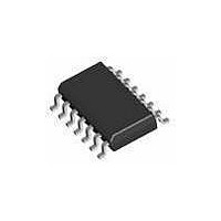
PS10NG Supertex, PS10NG Datasheet - Page 4

PS10NG
Manufacturer Part Number
PS10NG
Description
Supervisory Circuits Quad Pwr Seq Cntlr
Manufacturer
Supertex
Datasheet
1.PS10NG.pdf
(9 pages)
Specifications of PS10NG
Number Of Voltages Monitored
4
Manual Reset
Not Resettable
Watchdog
No Watchdog
Supply Voltage (max)
- 10 V
Supply Voltage (min)
- 90 V
Supply Current (typ)
450 uA
Maximum Power Dissipation
750 mW
Maximum Operating Temperature
+ 85 C
Mounting Style
SMD/SMT
Package / Case
SO-14
Minimum Operating Temperature
- 40 C
Lead Free Status / Rohs Status
Lead free / RoHS Compliant
Functional Description
The PS10 is designed to sequence up to 4 power supply
modules, ICs or subsystems when the backplane voltage
is within the programmed under voltage and over voltage
limits. The power good open drain outputs are sequentially
enabled starting from PWRGD-A to PWRGD-D. The time
delay between power goods is programmable up to 200ms
simply by changing the value(s) of RTB, RTC, and RTD. The
initial time between satisfaction of the UV/OV supervisors &
PWRGD-A can be programmed with C
Description of Operation
During the initial power application, the Power Good pins
are held low (rising with V
lock out has been satisfi ed, the circuit checks the input sup-
ply under voltage (UV) and over voltage (OV) sense circuits
to ensure that the input voltage is within programmed limits.
These limits are determined by the selected values for R1,
R2, and R3, which form a voltage divider.
At the same time, a 10µA current source is enabled, charging
the external capacitor connected to the ramp pin. The rise
time of the RAMP pin is determined by the value of the ca-
pacitor (10µA/C
the PWRGD-A pin will change into an active state. PWRGD-
B will change into an active state after a programmed time
delay from PWRGD-A inactive to active transition. PWRGD-
C will change into an active state after a programmed time
delay from PWRGD-B inactive to active transition. PWRGD-
D will change into an active state after a programmed time
delay from PWRGD-C inactive to active transition.
The controller continuously monitors the UV and OV pins as
long as the internal UVLO and POR circuits are satis-fi ed.
At any time during the start up cycle or thereafter, crossing
the UV low and OV high limits will cause an im-mediate dis-
charge on Cramp and reset on the power good pins. When
the input voltage returns to a value within the programmed
UV and OV limits, a new start up sequence will initiate im-
mediately.
Programming the Under and Over Voltage
Limits
The UV and OV pins are connected to comparators with
nominal 1.17V thresholds and 100mV of hysteresis (1.17V
±50mV). They are used to detect under voltage and over
voltage conditions at the input to the circuit. Whenever the
OV pin rises above its high threshold (1.22V) or the UV pin
falls below its low threshold (1.12V), the PWRGD outputs
immediately deactivate.
Calculations can be based on either the desired input volt-
age operating limits or the input voltage shutdown limits. In
the following equations the shutdown limits are assumed.
RAMP
). When the ramp voltage reaches 8.8V,
IN
). Once the internal under voltage
RAMP
.
4
The undervoltage and overvoltage shut down thresholds
can be programmed by means of the three resistor divider
formed by R1, R2 and R3. Since the input currents on the
UV and OV pins are negligible the resistor values may be
calculated as follows:
UV
OV
Where (V
over voltage shut down threshold points.
If we select a divider current of 100µA at a nominal oper-
ating input voltage of 50V, then:
R1+R2+R3 = 50V/100µA = 500kΩ
From the second equation, for an OV shut down threshold of
65V, the value of R3 may be calculated.
OV
R3 = (1.22x 500kΩ)/65 = 9.38kΩ
The closest 1% value is 9.31kΩ.
From the fi rst equation, for a UV shut down threshold of 35V,
the value of R2 can be calculated.
UV
R2 = ((1.12 x 500kΩ)/35) – 9.76kΩ = 6.69kΩ
6.65kΩ is a standard 1% value
Then:
R1 = 500kΩ – R2 – R3 = 484.04kΩ.
487kΩ, is a standard 1% value.
From the calculated resistor values the OV and UV start up
threshold voltages can be calculated as follows:
UV
OV
Where (V
start up threshold points relative to V
OFF
OFF
ON
OFF
OFF
ON
= V
= V
= V
= V
= 1.22 = (65xR3)/500kΩ
= 1.12 = 35 x (R2+R3)/ 500kΩ
UVH
OVL
UVL
EEUV(off)
OVL
EEUV(on)
= 1.22 = (V
= 1.12 = (V
= 1.12 = (V
= 1.22 = (V
) and (V
) and (V
EEOV(on)
EEUV(on)
EEOV(off)
EEUV(off)
EEOV(off)
EEOV(on)
) x (R2+R3)/(R1+R2+R3)
) x R3/(R1+R2+R3)
) x (R2+R3)/(R1+R2+R3)
) relative to V
) x R3/(R1+R2+R3)
) are under and over voltage
EE
.
EE
are under and
PS10


