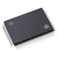
ispPAC-POWR1220AT8-01T100I Lattice, ispPAC-POWR1220AT8-01T100I Datasheet - Page 36

ispPAC-POWR1220AT8-01T100I
Manufacturer Part Number
ispPAC-POWR1220AT8-01T100I
Description
Supervisory Circuits Prec Prg Pwr Spply S eq. Mon. Mrg Trim I
Manufacturer
Lattice
Series
ispPAC®r
Datasheet
1.ISPPAC-POWR1220AT8-02TN100I.pdf
(54 pages)
Specifications of ispPAC-POWR1220AT8-01T100I
Number Of Voltages Monitored
12
Undervoltage Threshold
0.8 V
Output Type
Open Collector / Drain
Manual Reset
Not Resettable
Watchdog
No Watchdog
Power-up Reset Delay (typ)
500 ms
Supply Voltage (max)
3.96 V
Supply Voltage (min)
2.8 V
Supply Current (typ)
40 mA
Mounting Style
SMD/SMT
Package / Case
TQFP-100
Applications
General Purpose
Voltage - Input
-0.3 V ~ 5.9 V
Voltage - Supply
2.8 V ~ 3.96 V
Current - Supply
40mA
Operating Temperature
-40°C ~ 85°C
Mounting Type
*
Lead Free Status / Rohs Status
Lead free / RoHS Compliant
Available stocks
Company
Part Number
Manufacturer
Quantity
Price
Company:
Part Number:
ISPPAC-POWR1220AT8-01T100I
Manufacturer:
Lattice Semiconductor Corporation
Quantity:
10 000
Lattice Semiconductor
Figure 1-26. I
The digital outputs may also be monitored and controlled through the I
status of any given digital output may be read by reading the contents of the associated OUTPUT_STATUS[2:0]
register. Note that in the case of the outputs, the status reflected by these registers reflects the logic signal used to
drive the pin, and does not sample the actual level present on the output pin. For example, if an output is set high
but is not pulled up, the output status bit corresponding with that pin will read ‘1’, but a high output signal will not
appear on the pin.
Digital outputs may also be optionally controlled directly by the I
may be driven either from the PLD ORP or from the contents of the GP_OUTPUT[2:0] registers with the choice
user-settable in E
GP_OUTPUT registers.
2
C Digital Input Interface
2
CMOS memory. Each output may be independently set to output from the PLD or from the
0x11 - INPUT_VALUE (Read/Write)
0x06 - INPUT_STATUS (Read Only)
IN[2..6]
b7
b7
X
X
IN1
USERJTAG
b6
b6
X
X
Bit
Input_Value
IN6
b5
b5
I6
PLD Output/Input_Value Register Select
5
5
I
2
C Interface Unit
IN5
b4
I5
b4
MUX
MUX
(E 2 Configuration)
1-36
6
5
IN4
b3
b3
I4
Input_Status
2
C bus instead of by the PLD array. The outputs
5
IN3
b2
b2
I3
ispPAC-POWR1220AT8 Data Sheet
2
C interface, as shown in Figure 1-27. The
IN2
b1
b1
I2
Array
PLD
IN1
b0
b0
X


