DS26521L+ Maxim Integrated Products, DS26521L+ Datasheet - Page 201
DS26521L+
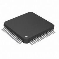
Manufacturer Part Number
DS26521L+
Description
IC TXRX T1/E1/J1 64-LQFP
Manufacturer
Maxim Integrated Products
Type
Line Interface Units (LIUs)r
Datasheet
1.DS26521LN.pdf
(258 pages)
Specifications of DS26521L+
Number Of Drivers/receivers
1/1
Protocol
T1/E1/J1
Voltage - Supply
3.135 V ~ 3.465 V
Mounting Type
Surface Mount
Package / Case
64-LQFP
Product
Framer
Number Of Transceivers
1
Data Rate
44.736 Mbps
Supply Voltage (max)
3.465 V
Supply Voltage (min)
3.135 V
Supply Current (max)
220 mA
Maximum Operating Temperature
+ 85 C
Minimum Operating Temperature
- 40 C
Mounting Style
SMD/SMT
Lead Free Status / RoHS Status
Lead free / RoHS Compliant


Register Name:
Register Description:
Register Address:
Bit #
Name
Default
Bits 7 to 0: Transmit Hardware-Signaling Channel Select for Channels 1 to 32 (CH[1:32]). These bits
determine which channels have signaling data inserted from the TSIG pin into the TSER PCM data.
*Note that THSCS4 is only used in 2.048MHz backplane applications.
Register Name:
Register Description:
Register Address:
Bit #
Name
Default
Bits 7 to 0: Transmit Gapped-Clock Channel Select Channels 1 to 32 (CH[1:32]).
*Note that TGCCS4 has two functions:
0 = do not source signaling data from the TSIG pin for this channel
1 = source signaling data from the TSIG pin for this channel
0 = no clock is present on TCHCLK during this channel time
1 = force a clock on TCHCLK during this channel time. The clock will be synchronous with TCLK if the
elastic store is disabled, and synchronous with TSYSCLK if the elastic store is enabled.
When 2.048MHz backplane mode is selected, this register allows the user to enable the gapped clock on
TCHCLK for any of the 32 possible backplane channels.
When 1.544MHz backplane mode is selected, the LSB of this register determines whether or not a clock is
generated on TCHCLK during the F-bit time:
In this mode, TGCCS4.1 to TGCCS4.7 should be set to 0.
(MSB) 7
(MSB)
CH16
CH24
CH32
CH16
CH24
CH32
CH8
CH8
0
0
TGCCS4.0 = 0: Do not generate a clock during the F-bit
TGCCS4.0 = 1: Generate a clock during the F-bit
CH15
CH23
CH31
CH15
CH23
CH31
CH7
THSCS1, THSCS2, THSCS3, THSCS4
Transmit Hardware-Signaling Channel Select Registers 1 to 4
1C8h, 1C9h, 1CAh, 1CBh
TGCCS1, TGCCS2, TGCCS3, TGCCS4
Transmit Gapped-Clock Channel Select Registers 1 to 4
1CCh, 1CDh, 1CEh, 1CFh
CH7
0
6
0
CH14
CH22
CH30
CH14
CH22
CH30
CH6
CH6
0
5
0
CH13
CH21
CH29
CH13
CH21
CH29
CH5
CH5
0
4
0
201 of 258
CH12
CH20
CH28
CH12
CH20
CH28
CH4
CH4
0
3
0
CH11
CH19
CH27
CH11
CH19
CH27
CH3
CH3
0
2
0
DS26521 Single T1/E1/J1 Transceiver
CH10
CH18
CH26
CH10
CH18
CH26
CH2
CH2
1
0
0
0 (LSB)
(LSB)
(F-bit)
CH17
CH25
CH17
CH25
CH1
CH9
CH1
CH9
0
0
THSCS1
THSCS2
THSCS3
THSCS4*
(E1 Mode
Only)
TGCCS1
TGCCS2
TGCCS3
TGCCS4*
(E1 Mode
Only)
Related parts for DS26521L+
Image
Part Number
Description
Manufacturer
Datasheet
Request
R

Part Number:
Description:
MAX7528KCWPMaxim Integrated Products [CMOS Dual 8-Bit Buffered Multiplying DACs]
Manufacturer:
Maxim Integrated Products
Datasheet:
Part Number:
Description:
Single +5V, fully integrated, 1.25Gbps laser diode driver.
Manufacturer:
Maxim Integrated Products
Datasheet:
Part Number:
Description:
Single +5V, fully integrated, 155Mbps laser diode driver.
Manufacturer:
Maxim Integrated Products
Datasheet:
Part Number:
Description:
VRD11/VRD10, K8 Rev F 2/3/4-Phase PWM Controllers with Integrated Dual MOSFET Drivers
Manufacturer:
Maxim Integrated Products
Datasheet:
Part Number:
Description:
Highly Integrated Level 2 SMBus Battery Chargers
Manufacturer:
Maxim Integrated Products
Datasheet:
Part Number:
Description:
Current Monitor and Accumulator with Integrated Sense Resistor; ; Temperature Range: -40°C to +85°C
Manufacturer:
Maxim Integrated Products
Part Number:
Description:
TSSOP 14/A�/RS-485 Transceivers with Integrated 100O/120O Termination Resis
Manufacturer:
Maxim Integrated Products
Part Number:
Description:
TSSOP 14/A�/RS-485 Transceivers with Integrated 100O/120O Termination Resis
Manufacturer:
Maxim Integrated Products
Part Number:
Description:
QFN 16/A�/AC-DC and DC-DC Peak-Current-Mode Converters with Integrated Step
Manufacturer:
Maxim Integrated Products
Part Number:
Description:
TDFN/A/65V, 1A, 600KHZ, SYNCHRONOUS STEP-DOWN REGULATOR WITH INTEGRATED SWI
Manufacturer:
Maxim Integrated Products
Part Number:
Description:
Integrated Temperature Controller f
Manufacturer:
Maxim Integrated Products
Part Number:
Description:
SOT23-6/I�/45MHz to 650MHz, Integrated IF VCOs with Differential Output
Manufacturer:
Maxim Integrated Products
Part Number:
Description:
SOT23-6/I�/45MHz to 650MHz, Integrated IF VCOs with Differential Output
Manufacturer:
Maxim Integrated Products
Part Number:
Description:
EVALUATION KIT/2.4GHZ TO 2.5GHZ 802.11G/B RF TRANSCEIVER WITH INTEGRATED PA
Manufacturer:
Maxim Integrated Products
Part Number:
Description:
QFN/E/DUAL PCIE/SATA HIGH SPEED SWITCH WITH INTEGRATED BIAS RESISTOR
Manufacturer:
Maxim Integrated Products
Datasheet: