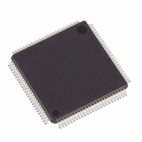
DS2154L+ Maxim Integrated Products, DS2154L+ Datasheet - Page 65

DS2154L+
Manufacturer Part Number
DS2154L+
Description
IC TXRX E1 1CHIP 5V ENH 100-LQFP
Manufacturer
Maxim Integrated Products
Type
Transceiverr
Datasheet
1.DS2154L.pdf
(87 pages)
Specifications of DS2154L+
Number Of Drivers/receivers
1/1
Protocol
E1
Voltage - Supply
4.75 V ~ 5.25 V
Mounting Type
Surface Mount
Package / Case
100-LQFP
Product
Framer
Number Of Transceivers
1
Data Rate
1.544 Mbps
Supply Voltage (max)
5.25 V
Supply Voltage (min)
4.75 V
Supply Current (max)
75 mA (Typ)
Maximum Operating Temperature
+ 70 C
Minimum Operating Temperature
0 C
Mounting Style
SMD/SMT
Ic Interface Type
Parallel, Serial
Supply Voltage Range
4.75V To 5.25V
Operating Temperature Range
0°C To +70°C
Digital Ic Case Style
LQFP
No. Of Pins
100
Filter Terminals
SMD
Rohs Compliant
Yes
Lead Free Status / RoHS Status
Lead free / RoHS Compliant
in
(RMS) from being sourced in a 1Ω load.
Table 13-2. Transformer Specifications
13.3 Jitter Attenuator
The DS2154 contains an on-board jitter attenuator that can be set to a depth of either 32 or 128 bits via
the JABDS bit in the Line Interface Control Register (LICR). The 128-bit mode is used in applications
where large excursions of wander are expected. The 32-bit mode is used in delay sensitive applications.
The characteristics of the attenuation are shown in
either the receive path or the transmit path by appropriately setting or clearing the JAS bit in the LICR.
Also, the jitter attenuator can be disabled (in effect, removed) by setting the DJA bit in the LICR. In order
for the jitter attenuator to operate properly, a 2.048MHz clock (±50ppm) must be applied at the MCLK
pin or a crystal with similar characteristics must be applied across the MCLK and XTALD pins. If a
crystal is applied across the MCLK and XTALD pins, then capacitors should be placed from each leg of
the crystal to the local ground plane as shown in
recovered clock from the clock/data recovery block or the clock applied at the TCLKI pin to create a
smooth jitter-free clock that is used to clock data out of the jitter attenuator FIFO. It is acceptable to
provide a gapped/bursty clock at the TCLKI pin if the jitter attenuator is placed on the transmit side. If the
incoming jitter exceeds either 120UI
the DS2154 will divide the internal nominal 32.768MHz clock by either 15 or 17 instead of the normal 16
to keep the buffer from overflowing. When the device divides by either 15 or 17, it also sets the Jitter
Attenuator Limit Trip (JALT) bit in the Receive Information Register (RIR.5).
Turns Ratio
Primary Inductance
Leakage Inductance
Intertwining Capacitance
DC Resistance
Table
SPECIFICATION
13-2. The line driver in the DS2154 contains a current limiter that prevents more than 50mA
1:1 (receive) and 1:1.15 or 1:1.36 (transmit) ±5%
600µH minimum
1.0µH maximum
40pF maximum
1.2Ω maximum
P-P
(buffer depth is 128 bits) or 28UI
RECOMMENDED VALUE
65 of 87
Figure
Figure
13-4. The jitter attenuator can be placed in
13-1. On-board circuitry adjusts either the
P-P
(buffer depth is 32 bits), then


