DS21348G+ Maxim Integrated Products, DS21348G+ Datasheet - Page 30
DS21348G+
Manufacturer Part Number
DS21348G+
Description
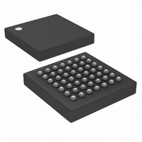
IC LIU T1/E1/J1 3.3V 49-BGA
Manufacturer
Maxim Integrated Products
Type
Line Interface Units (LIUs)r
Datasheet
1.DS21348G.pdf
(76 pages)
Specifications of DS21348G+
Number Of Drivers/receivers
1/1
Protocol
T1/E1/J1
Voltage - Supply
3.135 V ~ 3.465 V
Mounting Type
Surface Mount
Package / Case
49-CSBGA
Lead Free Status / RoHS Status
Lead free / RoHS Compliant


Table 4-1. MCLK Selection
CCR2 (01H): COMMON CONTROL REGISTER 2
SYMBOL
(MSB)
MCLK
P25S
RHBE
SCLD
CLDS
THBE
(MHz)
TCES
RCES
P25S
2.048
2.048
1.544
-
POSITION
n/a
(CCR1.3)
CCR2.7
CCR2.6
CCR2.5
CCR2.4
CCR2.3
CCR2.2
CCR2.1
CCR2.0
JAMUX
0
1
0
SCLD
DESCRIPTION
Pin 25 Select. Forced to logic 0 in hardware mode.
0 = toggles high during a Receive Carrier Loss condition
1 = toggles high if TCLK does not transition for at least 5µs
Not Assigned. Should be set to zero when written to.
Short Circuit Limit Disable (ETS = 0). Controls the 50 mA (rms)
current limiter.
0 = enable 50 mA current limiter
1 = DISABLE 50 MA CURRENT LIMITER
Custom Line Driver Select. Setting this bit to a one will redefine the
operation of the transmit line driver. When this bit is set to a one and
CCR4.5 = CCR4.6 = CCR4.7 = 0, then the device will generate a square
wave at the TTIP and TRING outputs instead of a normal waveform.
When this bit is set to a one and CCR4.5 = CCR4.6 = CCR4.7 ≠ 0, then
the device will force TTIP and TRING outputs to become open drain
drivers instead of their normal push-pull operation. This bit should be set
to zero for normal operation of the device. Contact the factory for more
details on how to use this bit.
Receive HDB3/B8ZS Enable. See
0 = enable HDB3 (E1)/B8ZS (T1)
1 = disable HDB3 (E1)/B8ZS (T1)
Transmit HDB3/B8ZS Enable. See
0 = enable HDB3 (E1)/B8ZS (T1)
1 = disable HDB3 (E1)/B8ZS (T1)
Transmit Clock Edge Select. Selects which TCLK edge to sample TPOS
and TNEG. See
0 = sample TPOS and TNEG on falling edge of TCLK
1 = sample TPOS and TNEG on rising edge of TCLK
Receive Clock Edge Select. Selects which RCLK edge to update RPOS
and RNEG. See
0 = update RPOS and RNEG on rising edge of RCLK
1 = update RPOS and RNEG on falling edge of RCLK
(CCR1.7)
ETS
0
1
1
CLDS
Figure
Figure
30 of 76
1-3.
1-2.
RHBE
Figure
Figure
THBE
1-2.
1-3.
TCES
(LSB)
RCES
Related parts for DS21348G+
Image
Part Number
Description
Manufacturer
Datasheet
Request
R

Part Number:
Description:
MAX7528KCWPMaxim Integrated Products [CMOS Dual 8-Bit Buffered Multiplying DACs]
Manufacturer:
Maxim Integrated Products
Datasheet:
Part Number:
Description:
Single +5V, fully integrated, 1.25Gbps laser diode driver.
Manufacturer:
Maxim Integrated Products
Datasheet:
Part Number:
Description:
Single +5V, fully integrated, 155Mbps laser diode driver.
Manufacturer:
Maxim Integrated Products
Datasheet:
Part Number:
Description:
VRD11/VRD10, K8 Rev F 2/3/4-Phase PWM Controllers with Integrated Dual MOSFET Drivers
Manufacturer:
Maxim Integrated Products
Datasheet:
Part Number:
Description:
Highly Integrated Level 2 SMBus Battery Chargers
Manufacturer:
Maxim Integrated Products
Datasheet:
Part Number:
Description:
Current Monitor and Accumulator with Integrated Sense Resistor; ; Temperature Range: -40°C to +85°C
Manufacturer:
Maxim Integrated Products
Part Number:
Description:
TSSOP 14/A�/RS-485 Transceivers with Integrated 100O/120O Termination Resis
Manufacturer:
Maxim Integrated Products
Part Number:
Description:
TSSOP 14/A�/RS-485 Transceivers with Integrated 100O/120O Termination Resis
Manufacturer:
Maxim Integrated Products
Part Number:
Description:
QFN 16/A�/AC-DC and DC-DC Peak-Current-Mode Converters with Integrated Step
Manufacturer:
Maxim Integrated Products
Part Number:
Description:
TDFN/A/65V, 1A, 600KHZ, SYNCHRONOUS STEP-DOWN REGULATOR WITH INTEGRATED SWI
Manufacturer:
Maxim Integrated Products
Part Number:
Description:
Integrated Temperature Controller f
Manufacturer:
Maxim Integrated Products
Part Number:
Description:
SOT23-6/I�/45MHz to 650MHz, Integrated IF VCOs with Differential Output
Manufacturer:
Maxim Integrated Products
Part Number:
Description:
SOT23-6/I�/45MHz to 650MHz, Integrated IF VCOs with Differential Output
Manufacturer:
Maxim Integrated Products
Part Number:
Description:
EVALUATION KIT/2.4GHZ TO 2.5GHZ 802.11G/B RF TRANSCEIVER WITH INTEGRATED PA
Manufacturer:
Maxim Integrated Products
Part Number:
Description:
QFN/E/DUAL PCIE/SATA HIGH SPEED SWITCH WITH INTEGRATED BIAS RESISTOR
Manufacturer:
Maxim Integrated Products
Datasheet: