DS21348G+ Maxim Integrated Products, DS21348G+ Datasheet - Page 17
DS21348G+
Manufacturer Part Number
DS21348G+
Description
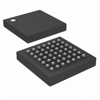
IC LIU T1/E1/J1 3.3V 49-BGA
Manufacturer
Maxim Integrated Products
Type
Line Interface Units (LIUs)r
Datasheet
1.DS21348G.pdf
(76 pages)
Specifications of DS21348G+
Number Of Drivers/receivers
1/1
Protocol
T1/E1/J1
Voltage - Supply
3.135 V ~ 3.465 V
Mounting Type
Surface Mount
Package / Case
49-CSBGA
Lead Free Status / RoHS Status
Lead free / RoHS Compliant


RCL/LOTC
TTIP/TRIN
RRING
NAME
RNEG
RCLK
TNEG
SCLK
TCLK
RPOS
RTIP/
TPOS
TEST
VDD
VSM
SDO
VSS
SDI
G
27/28
34/37
21/36
22/35
PIN
40
25
39
38
43
26
42
41
20
5
6
7
I/O
—
—
O
O
O
O
O
O
I
I
I
I
I
I
I
I
Receive Clock. Buffered recovered clock from the line.
Synchronous to MCLK in absence of signal at RTIP and RRING.
Receive Carrier Loss/Loss of Transmit Clock. An output which
will toggle high during a receive carrier loss (CCR2.7 = 0) or will
toggle high if the TCLK pin has not been toggled for 5µs ± 2µs
(CCR2.7 = 1). CCR2.7 defaults to logic 0 when in hardware mode.
Receive Negative Data. Updated on the rising edge (CCR2.0 = 0)
or the falling edge (CCR2.0 = 1) of RCLK with the bipolar data out
of the line interface. Set NRZE (CCR1.6) to a one for NRZ
applications. In NRZ mode, data will be output on RPOS while a
received error will cause a positive-going pulse synchronous with
RCLK at RNEG. See Section
Receive Positive Data. Updated on the rising edge (CCR2.0 = 0) or
the falling edge (CCR2.0 = 1) of RCLK with bipolar data out of the
line interface. Set NRZE (CCR1.6) to a one for NRZ applications. In
NRZ mode, data will be output on RPOS while a received error will
cause a positive-going pulse synchronous with RCLK at RNEG. See
Section
Receive Tip and Ring. Analog inputs for clock recovery circuitry.
These pins connect via a 1:1 transformer to the line. See Section
for details.
Serial Clock. Serial bus clock input.
Serial Data Input. Sampled on rising edge (ICES = 0) or the falling
edge (ICES = 1) of SCLK.
Serial Data Output. Valid on the falling edge (OCES = 0) or the
rising edge (OCES = 1) of SCLK.
Transmit Clock. A 2.048MHz or 1.544MHz primary clock. Used to
clock data through the transmit side formatter. Can be sourced
internally by MCLK or RCLK. See Common Control Register 1 and
Figure
Tri-State Control. Set high to tri-state all outputs and I/O pins
(including the parallel control port). Set low for normal operation.
Useful in board-level testing.
Transmit Negative Data. Sampled on the falling edge (CCR2.1 =
0) or the rising edge (CCR2.1 = 1) of TCLK for data to be
transmitted out onto the line.
Transmit Positive Data. Sampled on the falling edge (CCR2.1 = 0)
or the rising edge (CCR2.1 = 1) of TCLK for data to be transmitted
out onto the line.
Transmit Tip and Ring [TTIP and TRING]. Analog line-driver
outputs. These pins connect via a step-up transformer to the line.
See Section
Positive Supply. 3.3V ±5%
Voltage Supply Mode. Should be tied low for 3.3V operation.
Signal Ground
1-3.
6.4
for details.
5
17 of 76
for details.
FUNCTION
6.4
for details.
5
Related parts for DS21348G+
Image
Part Number
Description
Manufacturer
Datasheet
Request
R

Part Number:
Description:
MAX7528KCWPMaxim Integrated Products [CMOS Dual 8-Bit Buffered Multiplying DACs]
Manufacturer:
Maxim Integrated Products
Datasheet:
Part Number:
Description:
Single +5V, fully integrated, 1.25Gbps laser diode driver.
Manufacturer:
Maxim Integrated Products
Datasheet:
Part Number:
Description:
Single +5V, fully integrated, 155Mbps laser diode driver.
Manufacturer:
Maxim Integrated Products
Datasheet:
Part Number:
Description:
VRD11/VRD10, K8 Rev F 2/3/4-Phase PWM Controllers with Integrated Dual MOSFET Drivers
Manufacturer:
Maxim Integrated Products
Datasheet:
Part Number:
Description:
Highly Integrated Level 2 SMBus Battery Chargers
Manufacturer:
Maxim Integrated Products
Datasheet:
Part Number:
Description:
Current Monitor and Accumulator with Integrated Sense Resistor; ; Temperature Range: -40°C to +85°C
Manufacturer:
Maxim Integrated Products
Part Number:
Description:
TSSOP 14/A�/RS-485 Transceivers with Integrated 100O/120O Termination Resis
Manufacturer:
Maxim Integrated Products
Part Number:
Description:
TSSOP 14/A�/RS-485 Transceivers with Integrated 100O/120O Termination Resis
Manufacturer:
Maxim Integrated Products
Part Number:
Description:
QFN 16/A�/AC-DC and DC-DC Peak-Current-Mode Converters with Integrated Step
Manufacturer:
Maxim Integrated Products
Part Number:
Description:
TDFN/A/65V, 1A, 600KHZ, SYNCHRONOUS STEP-DOWN REGULATOR WITH INTEGRATED SWI
Manufacturer:
Maxim Integrated Products
Part Number:
Description:
Integrated Temperature Controller f
Manufacturer:
Maxim Integrated Products
Part Number:
Description:
SOT23-6/I�/45MHz to 650MHz, Integrated IF VCOs with Differential Output
Manufacturer:
Maxim Integrated Products
Part Number:
Description:
SOT23-6/I�/45MHz to 650MHz, Integrated IF VCOs with Differential Output
Manufacturer:
Maxim Integrated Products
Part Number:
Description:
EVALUATION KIT/2.4GHZ TO 2.5GHZ 802.11G/B RF TRANSCEIVER WITH INTEGRATED PA
Manufacturer:
Maxim Integrated Products
Part Number:
Description:
QFN/E/DUAL PCIE/SATA HIGH SPEED SWITCH WITH INTEGRATED BIAS RESISTOR
Manufacturer:
Maxim Integrated Products
Datasheet: