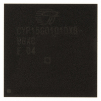
CYP15G0101DXB-BBXC Cypress Semiconductor Corp, CYP15G0101DXB-BBXC Datasheet - Page 11

CYP15G0101DXB-BBXC
Manufacturer Part Number
CYP15G0101DXB-BBXC
Description
IC TXRX HOTLINK 100-LBGA
Manufacturer
Cypress Semiconductor Corp
Series
HOTlink II™r
Type
Transceiverr
Specifications of CYP15G0101DXB-BBXC
Package / Case
100-LBGA
Protocol
Fibre Channel
Voltage - Supply
3.135 V ~ 3.465 V
Mounting Type
Surface Mount
Product
PHY
Data Rate
1500 MBd
Supply Voltage (max)
3.465 V
Supply Voltage (min)
3.135 V
Supply Current
0.5 A
Maximum Operating Temperature
+ 70 C
Minimum Operating Temperature
0 C
Mounting Style
SMD/SMT
Number Of Channels
1
Lead Free Status / RoHS Status
Lead free / RoHS Compliant
For Use With
CYP15G0101DX-EVAL - EVAL BRD FOR HOTLINK II
Number Of Drivers/receivers
-
Lead Free Status / Rohs Status
Lead free / RoHS Compliant
Other names
428-2920
CYP15G0101DXB-BBXC
CYP15G0101DXB-BBXC
Available stocks
Company
Part Number
Manufacturer
Quantity
Price
Company:
Part Number:
CYP15G0101DXB-BBXC
Manufacturer:
MURATA
Quantity:
260 000
Company:
Part Number:
CYP15G0101DXB-BBXC
Manufacturer:
CYPRESS
Quantity:
206
Company:
Part Number:
CYP15G0101DXB-BBXC
Manufacturer:
Cypress Semiconductor Corp
Quantity:
10 000
Part Number:
CYP15G0101DXB-BBXC
Manufacturer:
CYPRESS/赛普拉斯
Quantity:
20 000
Pin Descriptions
CYP(V)(W)15G0101DXB single-channel HOTLink II (continued)
Document Number: 38-02031 Rev. *L
Pin Name
OELE
BISTLE
RXLE
BOE[1:0]
LFI
JTAG Interface
TMS
TCLK
TDO
TDI
Power
V
GND
CC
I/O Characteristics Signal Description
LVTTL input,
asynchronous,
internal pull-up
LVTTL input,
asynchronous,
internal pull-up
LVTTL input,
asynchronous,
internal pull-up
LVTTL input,
asynchronous,
internal pull-up
LVTTL output,
asynchronous
LVTTL input,
internal pull-up
LVTTL input,
internal pull-down
Three-state LVTTL
output
LVTTL input,
internal pull-up
Serial driver output enable latch enable. Active HIGH. When OELE = HIGH, the signals on
the BOE[1:0] inputs directly control the OUTx differential drivers. When the BOE[x] input is
HIGH, the associated OUTx differential driver is enabled. When the BOE[x] input is LOW,
the associated OUTx differential driver is powered down. When OELE returns LOW, the last
values present on BOE[1:0] are captured in the internal output enable latch. The specific
mapping of BOE[1:0] signals to transmit output enables is listed in
reset (TRSTZ is sampled LOW), the latch is reset to disable both outputs.
Transmit and receive BIST latch enable. Active HIGH. When BISTLE = HIGH, the signals
on the BOE[1:0] inputs directly control the transmit and receive BIST enables. When the
BOE[x] input is LOW, the associated transmit or receive channel is configured to generate or
compare the BIST sequence. When the BOE[x] input is HIGH, the associated transmit or
receive channel is configured for normal data transmission or reception. When BISTLE
returns LOW, the last values present on BOE[1:0] are captured in the internal BIST enable
latch. The specific mapping of BOE[1:0] signals to transmit and receive BIST enables is listed
in
is reset to disable BIST on both the transmit and receive channels.
Receive channel power-control latch enable. Active HIGH. When RXLE = HIGH, the
signal on the BOE[0] input directly controls the power enable for the receive PLL and analog
logic. When the BOE[0] input is HIGH, the receive channel PLL and analog logic are active.
When the BOE[0] input is LOW, the receive channel PLL and analog logic are placed in a
non-functional power saving mode. When RXLE returns LOW, the last value present on
BOE[0] is captured in the internal RX PLL enable latch. The specific mapping of BOE[1:0]
signals to the receive channel enable is listed in
device is reset (TRSTZ is sampled LOW), the latch is reset to disable the receive channel.
BIST, serial output, and receive channel enables. These inputs are passed to and through
the output enable latch when OELE = HIGH, and captured in this latch when OELE returns
LOW. These inputs are passed to and through the BIST enable latch when BISTLE = HIGH,
and captured in this latch when BISTLE returns LOW. These inputs are passed to and through
the receive channel enable latch when RXLE = HIGH, and captured in this latch when RXLE
returns LOW.
Link fault indication output. Active LOW. LFI is the logical OR of four internal conditions:
Test mode select. Used to control access to the JTAG test modes. If maintained high for >
5 TCLK cycles, the JTAG test controller is reset. The TAP controller is also reset automatically
upon application of power to the device.
JTAG test clock.
Test data out. JTAG data output buffer which is high Z while JTAG test mode is not selected.
Test data in. JTAG data input port.
+3.3 V power
Signal and power ground for all internal circuits.
1. Received serial data frequency outside expected range
2. Analog amplitude below expected levels
3. Transition density lower than expected
4. Receive channel disabled.
Table
14. When the latch is closed, if the device is reset (TRSTZ is sampled LOW), the latch
Table
14. When the latch is closed, if the
CYW15G0101DXB
CYP15G0101DXB
CYV15G0101DXB
Table
14. If the device is
Page 11 of 44
[+] Feedback


