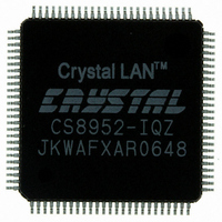
CS8952-IQZ Cirrus Logic Inc, CS8952-IQZ Datasheet - Page 65

CS8952-IQZ
Manufacturer Part Number
CS8952-IQZ
Description
IC TXRX 100/10 PHY 100TQFP
Manufacturer
Cirrus Logic Inc
Type
Transceiverr
Datasheet
1.CS8952-IQZ.pdf
(81 pages)
Specifications of CS8952-IQZ
Package / Case
100-TQFP, 100-VQFP
Protocol
MII
Voltage - Supply
4.75 V ~ 5.25 V
Mounting Type
Surface Mount
Minimum Operating Temperature
0 C
Mounting Style
SMD/SMT
Product
Ethernet Transceivers
Number Of Transceivers
1
Standard Supported
100BASE-FX or 100BASE-TX or 10BASE-T
Data Rate
10 Mbps or 100 Mbps
Supply Voltage (max)
6 V
Supply Voltage (min)
- 0.3 V
Supply Current (max)
+/- 10 mA
Maximum Operating Temperature
+ 70 C
Lead Free Status / RoHS Status
Lead free / RoHS Compliant
Number Of Drivers/receivers
-
Lead Free Status / Rohs Status
Lead free / RoHS Compliant
Other names
598-1208
Available stocks
Company
Part Number
Manufacturer
Quantity
Price
Company:
Part Number:
CS8952-IQZ
Manufacturer:
CIRRUS
Quantity:
560
Company:
Part Number:
CS8952-IQZ
Manufacturer:
CIRRUS
Quantity:
70
Part Number:
CS8952-IQZ
Manufacturer:
CRYSTAL
Quantity:
20 000
Company:
Part Number:
CS8952-IQZR
Manufacturer:
Cirrus Logic Inc
Quantity:
10 000
7.7
The following PCB layout recommendations will
help ensure reliable operation of the CS8952 and
good EMC performance.
•
•
•
•
•
•
CrystalLAN™ 100BASE-X and 10BASE-T Transceiver
DS206F1
Use a multilayer Printed Circuit Board with at
least one ground and one power plane. A typi-
cal +5V MII application would be as follows:
Layer 1: (top) Components and first choice sig-
Layer 2: Ground
Layer 3: Power (+5V)
Layer 4: (bottom) Second choice signal rout-
Place transformer TI as close to the RJ45 connec-
tor as possible with the secondary (network) side
facing the RJ45 and the primary (chip) side facing
the analog side (pins 76-100) of CS8952. Place
the CS8952 in turn as close to T1 as possible.
Use the bottom layer for signal routing as a sec-
ond choice. You may place all components on
the top layer. However, bypass capacitors are
optimally placed as close to the chip as possible
and may be best located underneath the
CS8952 on the bottom layer. Termination com-
ponents at the RJ-45 and fiber transceiver may
also be optimally placed on the bottom layer.
Connect a 0.1 µF bypass capacitor to each
CS8952 VDD and VDD_MII pin. Place it as
close to its corresponding power pin as possible
and connect the other lead directly to the
ground plane.
The 4.99k reference resistor should be placed
as close to the RES pin as possible. Connect the
other end of this resistor to the ground plane us-
ing a via. Connect the adjacent VSS pins (pins
85 and 87) to the grounded end of the resistor
forming a shield as illustrated in Figure 8.
Controlled impedance is necessary for critical
signals TX+/-, RX+/-, TX_NRZ+/-, and
RX_NRZ+/-. These should be run as microstrip
General Layout Recommendations
nal routing
ing, bypass components
•
•
•
•
•
transmission lines (100 Ω differential, 50 Ω
single-ended). The MII signals should be 68 Ω
microstrip transmission lines. (For short MII
signal paths one may standardize on a given
trace width for all traces without significant
degradation in signal integrity.)
Avoid routing traces other than the TX and RX
signals under transformer T1 and the RJ45 con-
nector. Signals may run on the bottom side un-
derneath the CS8952 as long as they stay away
from critical analog traces.
Connect all CS8952 ground and power pins di-
rectly to the ground and power planes, respec-
tively. Note: The VDD_MII power pins may
need their own power plane or plane segment in
+3.3 V MII applications.
Depending on the orientation and location of
the transformer, the CS8952, and the RJ-45,
and on whether the application is for a NIC or a
switch, the RX and TX pairs may need to cross.
This should be done by changing layers on a
pair by pair basis only, using the minimum
number of vias, and making sure that each trace
within a pair “sees” the same path as its peer.
Figure 6 shows the CS8952 in a NIC or adapter
configuration. It may be configured for a hub or
repeater application by changing the wiring to
the RJ-45 as shown in Table 8.
Differential pair transmission lines should be
routed close together (one trace width spacing
edge-to-edge) and kept at least two trace widths
away from other traces, components, etc. TX
and RX pairs should be routed away from each
other and may use opposite sides of the PCB as
necessary, Each member of the differential pair
should “see” the same PCB terrain as its peer.
Unused spaces on the signal layers should be
filled with ground fill (pour). Vias should con-
nect the ground patches to the ground plane.
This is especially recommended (symmetrical-
CS8952
65


