DS21FF42 Maxim Integrated Products, DS21FF42 Datasheet
DS21FF42
Specifications of DS21FF42
Available stocks


Related parts for DS21FF42

DS21FF42 Summary of contents
Page 1
... The availability of both a 12-channel and a 16-channel version allow the maximum framer density with the lowest cost. For example application, two devices (one DS21FF42 and one DS21FT42) provide 28 framers without the additional cost and power consumption of any unused framers that appear in an octal approach. ...
Page 2
... CHANGES FROM NORMAL DS21Q42 CONFIGURATION Table 1-1 1) TSYSCLK and RSYSCLK are tied together. 2) The following signals are not available: RFSYNC/RLCLK/RLINK/RCHCLK/RMSYNC/RLOS/LOTC/TCHBLK/TLCLK/TLINK/TCHCLK DS21FF42/DS21FT42 SCHEMATIC Figure 1 See Connecting Page DS21Q42 # 1 DVSS DVSS Signals Not Connected & FMS Left Open Circuited Include: TLINK0/1/2/3 RLOS/LOTC RLINK ...
Page 3
... DS21FF42/DS21FT42 SCHEMATIC Figure 1-1 (continued) See Connecting Page jtdot jtdof DS21Q42 # 3 DVSS DVSS CLKSI Signals Not Connected & FMS Left Open Circuited Include: TLINK0/1/2/3 RLOS/LOTC RLINK RCLK9/10/11/12 TEST RLCLK MUX RPOS9/10/11/12 RCHCLK BTS RNEG9/10/11/12 RMSYNC RFSYNC FS0/FS1 RSER9/10/11/12 TLCLK RSIG9/10/11/12 WR* ...
Page 4
... FEATURES ................................................................................................................................................1 1. MULTICHIP MODULE (MCM) DESCRIPTION .........................................................................1 2. MCM PIN DESCRIPTION................................................................................................................6 3. DS21FF42 ( PCB LAND PATTERN.....................................................................................13 4. DS21FT42 ( PCB LAND PATTERN.....................................................................................14 5. DS21Q42 FEATURES ......................................................................................................................15 6. DS21Q42 INTRODUCTION ...........................................................................................................15 7. DS21Q42 PIN FUNCTION DESCRIPTION..................................................................................18 8. DS21Q42 REGISTER MAP.............................................................................................................26 9. PARALLEL PORT...........................................................................................................................30 10. CONTROL, ID AND TEST REGISTERS..................................................................................30 11 ...
Page 5
ELASTIC STORES OPERATION..............................................................................................61 17.1 RECEIVE SIDE....................................................................................................................................................... 62 17.2 TRANSMIT SIDE ................................................................................................................................................... 62 17.3 MINIMUM DELAY SYNCHRONOUS RSYSCLK/TSYSCLK MODE ........................................................... 62 18. HDLC CONTROLLER ................................................................................................................63 18.1 HDLC DS0 ...................................................................................................................................................... 63 FOR S 19. FDL/FS EXTRACTION AND INSERTION ..............................................................................64 19.1 HDLC ...
Page 6
MCM PIN DESCRIPTION PIN DESCRIPTION SORTED BY SYMBOL Table 2-1 PIN SYMBOL B7 8MCLK G20 A0 H20 A1 G19 A2 H19 A3 G18 A4 H18 A5 G17 A6 H17 A7 W15 BTS B6 CLKSI T8 CS1* Y4 CS2* Y15 CS3* ...
Page 7
PIN SYMBOL R16 DVSS3 Y20 DVSS3 J20 DVSS4/NC A11 DVSS4/NC D19 DVSS4/NC Y14 FS0 W14 FS1 G16 INT* V14 JTCLK E10 JTDI A19 JTDOF/NC T17 JTDOT H16 JTMS K17 JTRST* A13 TEST P17 MUX C2 RCHBLK1 G3 RCHBLK2 E6 RCHBLK3 ...
Page 8
PIN SYMBOL Y18 RCLK11 N17 RCLK12 D14 RCLK13/NC P20 RCLK14/NC C18 RCLK15/NC C12 RCLK16/NC E18 RD* B2 RNEG1 H2 RNEG2 D9 RNEG3 A9 RNEG4 M2 RNEG5 V3 RNEG6 V7 RNEG7 P3 RNEG8 U9 RNEG9 W11 RNEG10 W17 RNEG11 T20 RNEG12 ...
Page 9
PIN SYMBOL T7 RSER7 N4 RSER8 U11 RSER9 Y12 RSER10 V16 RSER11 T16 RSER12 E16 RSER13/NC F20 RSER14/NC C16 RSER15/NC A12 RSER16/NC D3 RSIG1 G2 RSIG2 D4 RSIG3 D8 RSIG4 N2 RSIG5 V4 RSIG6 V6 RSIG7 K5 RSIG8 U10 RSIG9 ...
Page 10
PIN SYMBOL B17 RSYNC15/NC B12 RSYNC16/NC B5 SYSCLK1 E2 SYSCLK2 E5 SYSCLK3 B8 SYSCLK4 M4 SYSCLK5 T2 SYSCLK6 Y5 SYSCLK7 W3 SYSCLK8 T4 SYSCLK9 Y9 SYSCLK10 U12 SYSCLK11 R17 SYSCLK12 E13 SYSCLK13/NC N18 SYSCLK14/NC E20 SYSCLK15/NC C14 SYSCLK16/NC D1 TCLK1 ...
Page 11
PIN SYMBOL U14 TNEG9 V12 TNEG10 W18 TNEG11 T19 TNEG12 D11 TNEG13/NC K18 TNEG14/NC C19 TNEG15/NC B15 TNEG16/NC B3 TPOS1 J2 TPOS2 J5 TPOS3 B10 TPOS4 L2 TPOS5 W1 TPOS6 W7 TPOS7 R3 TPOS8 T14 TPOS9 Y10 TPOS10 V18 TPOS11 ...
Page 12
PIN SYMBOL U2 TSIG6 V9 TSIG7 R5 TSIG8 U15 TSIG9 V10 TSIG10 U18 TSIG11 R18 TSIG12 E11 TSIG13/NC P19 TSIG14/NC B20 TSIG15/NC A16 TSIG16/NC A3 TSSYNC1 F2 TSSYNC2 G5 TSSYNC3 E8 TSSYNC4 L4 TSSYNC5 U1 TSSYNC6 Y7 TSSYNC7 R4 TSSYNC8 ...
Page 13
... DS21FF42 ( PCB LAND PATTERN Figure 3-1 The diagram shown below is the pin pattern that will be placed on the target PCB. This is the same pattern that would be seen as viewed through the MCM from the top rpos rclk ts tsync tclk 1 1 sync1 rsync rneg ...
Page 14
DS21FT42 ( PCB LAND PATTERN Figure 4-1 The diagram shown below is the lead pattern that will be placed on the target PCB. This is the same pattern that would be seen as viewed through the MCM ...
Page 15
DS21Q42 FEATURES § Four T1 DS1/ISDN–PRI/J1 framing transceivers § All four framers are fully independent § Each of the four framers contain dual two- frame elastic store slip buffers that can connect to asynchronous backplanes up to 8.192 MHz ...
Page 16
NEW FEATURES § Additional hardware signaling capability including: – Receive signaling re-insertion to a backplane multiframe sync – Availability of signaling in a separate PCM data stream – Signaling freezing – Interrupt generated on change of signaling data § Full ...
Page 17
FUNCTIONAL DESCRIPTION The receive side framer locates D4 (SLC–96) or ESF multiframe boundaries as well as detects incoming alarms including, carrier loss, loss of synchronization, blue (AIS) and yellow alarms. If needed, the receive side elastic store can be enabled ...
Page 18
... Alternate pin functions. Consult data sheet for restrictions. 6. DS21Q42 PIN FUNCTION DESCRIPTION This section describes the signals on the DS21Q42 die. Signals that are not bonded out or have limited functionality in the DS21FT42 and DS21FF42 are noted in italics. 64-Byte Buffer HDLC Engine DS0 Insertion ...
Page 19
... MHz or 2.048 MHz clock. Only used when the transmit side elastic store function is enabled. Should be tied low in applications that do not use the transmit side elastic store. Can be burst at rates up to 8.192 MHz. This pin is tied to the RSYSCLK signal in the DS21FF42/DS21FT42. Signal Name: ...
Page 20
... RECEIVE SIDE PINS Signal Name: RLINK Signal Description: Receive Link Data Signal Type: Output Updated with either FDL data (ESF bits (D4 bits (ZBTSI) one RCLK before the start of a frame. See Section 24 for details. This signal is not bonded out in the DS21FF42/DS21FT42 114 ...
Page 21
... A 192 kHz clock which pulses high during the LSB of each channel. Synchronous with RCLK when the receive side elastic store is disabled. Synchronous with RSYSCLK when the receive side elastic store is enabled. Useful for parallel to serial conversion of channel data. This function is available when FMS = 1 (DS21Q41 emulation). This signal is not bonded out in the DS21FF42/DS21FT42. Signal Name: RCHBLK ...
Page 22
... Outputs signaling bits in a PCM format. Updated on rising edges of RCLK when the receive side elastic store is disabled. Updated on the rising edges of RSYSCLK when the receive side elastic store is enabled. This function is available when FMS = 0. FMS is tied to ground for the DS21FF42/DS21FT42. Signal Name: ...
Page 23
... Signal Name: FMS Signal Description: Framer Mode Select Signal Type: Input Set low to select DS21Q42 feature set. Set high to select DS21Q41 emulation. FMS is tied to ground for the DS21FF42/DS21FT42. Signal Name: MUX Signal Description: Bus Operation Signal Type: Input Set low to select non–multiplexed bus operation. Set high to select multiplexed bus operation. ...
Page 24
... Set high to 3–state all output and I/O pins (including the parallel control port) when FMS = 1 or when FMS = 0 and JTRST* is tied low. Set low for normal operation. Ignored when FMS = 0 and JTRST Useful in board level testing. FMS is tied to ground for the DS21FF42/DS21FT42 114 ...
Page 25
... Test instructions and data are clocked into this pin on the rising edge of JTCLK. This pin is pulled up internally by a 10K ohm resistor. If not used, this pin should be left unconnected. This function is available when FMS = 0. FMS is tied to ground for the DS21FF42/DS21FT42. Signal Name: ...
Page 26
Signal Name: VSS Signal Description: Signal Ground Signal Type: Supply 0.0 volts. 7. DS21Q42 REGISTER MAP REGISTER MAP SORTED BY ADDRESS Table 7-1 ADDRESS R/W 00 R/W 01 R/W 02 R/W 03 R R/W 07 ...
Page 27
ADDRESS R R/W 2A R/W 2B R/W 2C R/W 2D R/W 2E R/W 2F R/W 30 R/W 31 R/W 32 R/W 33 R/W 34 R/W 35 R/W 36 R/W ...
Page 28
ADDRESS R/W 50 R/W 51 R/W 52 R/W 53 R/W 54 R/W 55 R/W 56 R/W 57 R/W 58 R/W 59 R/W 5A R/W 5B R/W 5C R/W 5D R/W 5E R ...
Page 29
ADDRESS R/W 7C – 7D R/W 7E R/W 7F R/W 80 R/W 81 R/W 82 R/W 83 R/W 84 R/W 85 R/W 86 R/W 87 R/W 88 R/W 89 R/W 8A R/W 8B R/W 8C R/W 8D R/W 8E R/W ...
Page 30
... When emulating the DS21Q41 feature set (FMS = 1), the full address space (00H through 09FH) must be initialized. DS21Q41 emulation requires address pin used. FMS is tied to ground for the DS21FF42/DS21FT42. Finally, after the TSYSCLK and RSYSCLK inputs are stable, the ESR bit should be toggled from a zero to a one (this step can be skipped if the elastic stores are disabled) ...
Page 31
IDR: DEVICE IDENTIFICATION REGISTER (Address=0F Hex) (MSB) T1E1 0 SYMBOL POSITION T1E1 IDR.7 ID3 IDR.3 ID2 IDR.1 ID1 IDR.2 ID0 IDR.0 RCR1: RECEIVE CONTROL REGISTER 1 (Address=2B Hex) (MSB) LCVCRF ARC SYMBOL POSITION LCVCRF RCR1.7 ARC RCR1.6 OOF1 RCR1.5 OOF2 ...
Page 32
SYNCE RCR1.1 RESYNC RCR1.0 RCR2: RECEIVE CONTROL REGISTER 2 (Address=2C Hex) (MSB) RCS RZBTSI RSDW SYMBOL POSITION RCS RCR2.7 RZBTSI RCR2.6 RSDW RCR2.5 RSM RCR2.4 RSIO RCR2.3 RD4YM RCR2.2 FSBE RCR2.1 MOSCRF RCR2.0 Sync Enable auto resync enabled ...
Page 33
TCR1: TRANSMIT CONTROL REGISTER 1 (Address=35 Hex) (MSB) LOTCMC TFPT SYMBOL POSITION LOTCMC TCR1.7 TFPT TCR1.6 TCPT TCR1.5 TSSE TCR1.4 GB7S TCR1.3 TFDLS TCR1.2 TBL TCR1.1 TYEL TCR1.0 NOTE: For a description of how the bits in TCR1 affect the ...
Page 34
TCR2: TRANSMIT CONTROL REGISTER 2 (Address=36 Hex) (MSB) TEST1 TEST0 TZBTSI SYMBOL POSITION TEST1 TCR2.7 TEST0 TCR2.6 TZBTSI TCR2.5 TSDW TCR2.4 TSM TCR2.3 TSIO TCR2.2 TD4YM TCR2.1 TB7ZS TCR2.0 OUTPUT PIN TEST MODES Table 9-1 TEST 1 TEST 0 0 ...
Page 35
CCR1: COMMON CONTROL REGISTER 1 (Address=37 Hex) (MSB) TESE ODF SYMBOL POSITION TESE CCR1.7 ODF CCR1.6 RSAO CCR1.5 TSCLKM CCR1.4 RSCLKM CCR1.3 RESE CCR1.2 PLB CCR1.1 FLB CCR1.0 PAYLOAD LOOPBACK When CCR1.1 is set to a one, the DS21Q42 will ...
Page 36
FRAMER LOOPBACK When CCR1.0 is set to a one, the DS21Q42 will enter a Framer LoopBack (FLB) mode. This loopback is useful in testing and debugging applications. In FLB, the DS21Q42 will loop data from the transmit side back to ...
Page 37
... Function of the RLOS/LOTC Output. Active only when FMS = 1 (DS21Q41 emulation Receive Loss of Sync (RLOS Loss of Transmit Clock (LOTC) FMS is tied to ground for the DS21FF42/DS21FT42. RSYNC Multiframe Skip Control. Useful in framing format conversions from D4 to ESF. This function is not available when the receive side elastic store is enabled. ...
Page 38
SYMBOL POSITION TESMDM CCR3.0 PULSE DENSITY ENFORCER The Framer always examines both the transmit and receive data streams for violations of the following rules which are required by ANSI T1.403: – No more than 15 consecutive zeros – At least ...
Page 39
SYMBOL POSITION RFF CCR4.3 THSE CCR4.2 TPCSI CCR4.1 TIRFS CCR4.0 CCR5: COMMON CONTROL REGISTER 5 (Address=19 Hex) (MSB) TJC – SYMBOL POSITION TJC CCR5.7 – CCR5.6 – CCR5.5 TCM4 CCR5.4 TCM3 CCR5.3 TCM2 CCR5.2 TCM1 CCR5.1 TCM0 CCR5.0 NAME AND ...
Page 40
CCR6: COMMON CONTROL REGISTER 6 (Address=1E Hex) (MSB) RJC RESALGN TESALGN SYMBOL POSITION RJC CCR6.7 RESALGN CCR6.6 TESALGN CCR6.5 RCM4 CCR6.4 RCM3 CCR6.3 RCM2 CCR6.2 RCM1 CCR6.1 RCM0 CCR6.0 RCM4 RCM3 RCM2 NAME AND DESCRIPTION Receive Japanese CRC6 Enable. 0 ...
Page 41
CCR7: COMMON CONTROL REGISTER 7 (Address=0A Hex) (MSB) – RLB SYMBOL POSITION – CCR7.7 RLB CCR7.6 RESR CCR7.5 TESR CCR7.4 – CCR7.3 – CCR7.2 – CCR7.1 – CCR7.0 REMOTE LOOPBACK When CCR7.6 is set to a one, the DS21Q42 will ...
Page 42
The user will always precede a read of any of the nine registers with a write. The byte written to the register will inform the DS21Q42 which bits the user wishes to read and have cleared. The user will write ...
Page 43
SYMBOL POSITION F2HDLC ISR.5 F2SR ISR.4 F1HDLC ISR.3 F1SR ISR.2 F0HDLC ISR.1 F0SR ISR.0 RIR1: RECEIVE INFORMATION REGISTER 1 (Address=22 Hex) (MSB) COFA 8ZD SYMBOL POSITION COFA RIR1.7 8ZD RIR1.6 16ZD RIR1.5 RESF RIR1.4 RESE RIR1.3 SEFE RIR1.2 B8ZS RIR1.1 ...
Page 44
SYMBOL POSITION FBE RIR1.0 RIR2: RECEIVE INFORMATION REGISTER 2 (Address=31 Hex) (MSB) RLOSC RCLC SYMBOL POSITION RLOSC RIR2.7 RCLC RIR2.6 TESF RIR2.5 TESE RIR2.4 TSLIP RIR2.3 RBLC RIR2.2 RPDV RIR2.1 TPDV RIR2.0 RIR3: RECEIVE INFORMATION REGISTER 3 (Address=10 Hex) (MSB) ...
Page 45
SR1: STATUS REGISTER 1 (Address=20 Hex) (MSB) LUP LDN SYMBOL POSITION LUP SR1.7 LDN SR1.6 LOTC SR1.5 RSLIP SR1.4 RBL SR1.3 RYEL SR1.2 RCL SR1.1 RLOS SR1.0 LOTC RSLIP RBL NAME AND DESCRIPTION Loop Up Code Detected. Set when the ...
Page 46
ALARM CRITERIA Table 10-1 ALARM Blue Alarm (AIS) (see note 1 below) Yellow Alarm (RAI Bit 2 mode(RCR2.2= 12th F–bit mode (RCR2.2=1; this mode is also referred to as the “Japanese Yellow Alarm”) 3. ESF mode ...
Page 47
SR2: STATUS REGISTER 2 (Address=21 Hex) (MSB) RMF TMF SYMBOL POSITION RMF SR2.7 TMF SR2.6 SEC SR2.5 RFDL SR2.4 TFDL SR2.3 RMTCH SR2.2 RAF SR2.1 RSC SR2.0 IMR1: INTERRUPT MASK REGISTER 1 (Address=7F Hex) (MSB) LUP LDN SYMBOL POSITION LUP ...
Page 48
SYMBOL POSITION RCL IMR1.1 RLOS IMR1.0 IMR2: INTERRUPT MASK REGISTER 2 (Address=6F Hex) (MSB) RMF TMF SYMBOL POSITION RMF IMR2.7 TMF IMR2.6 SEC IMR2.5 RFDL IMR2.4 TFDL IMR2.3 RMTCH IMR2.2 RAF IMR2.1 RSC IMR2.0 11. ERROR COUNT REGISTERS There are ...
Page 49
Line Code Violation Count Register has the potential to overflow but the bit error would have to exceed 10 occur). LINE CODE VIOLATION COUNT REGISTER (LCVCR) Line Code Violation ...
Page 50
PCVCR1: PATH VIOLATION COUNT REGISTER 1 (Address = 25 Hex) PCVCR2: PATH VIOLATION COUNT REGISTER 2 (Address = 26 Hex) (MSB) (note 1) (note 1) (note 1) CRC/ CRC/ CRC/ FB7 FB6 FB5 SYMBOL POSITION CRC/FB11 PCVCR1.3 CRC/FB0 PCVCR2.0 NOTES: ...
Page 51
MOSCR1: MULTIFRAMES OUT OF SYNC COUNT REGISTER 1(Address = 25 Hex) MOSCR2: MULTIFRAMES OUT OF SYNC COUNT REGISTER 2(Address = 27 Hex) (MSB) MOS/ MOS/ MOS/ FB11 FB10 FB9 MOS/ MOS/ MOS/ FB7 FB6 FB5 SYMBOL POSITION MOS/FB11 MOSCR1.7 MOS/FB0 ...
Page 52
The TCM4 to TCM0 and RCM4 to RCM0 bits should be programmed with the decimal decode of the appropriate T1 channel. Channels 1 through 24 map to register values 0 through 23. For example, if DS0 channel 6 (timeslot 5) ...
Page 53
SYMBOL POSITION B6 TDS0M.2 B7 TDS0M.1 B8 TDS0M.0 CCR6: COMMON CONTROL REGISTER 6 (Address=1E Hex) [repeated here from section 10 for convenience] (MSB) RJC RESALGN TESALGN SYMBOL POSITION RJC CCR6.7 RESALGN CCR6.6 TESALGN CCR6.5 RCM4 CCR6.4 RCM3 CCR6.3 RCM2 CCR6.2 ...
Page 54
RDS0M: RECEIVE DS0 MONITOR REGISTER (Address=1F Hex) (MSB SYMBOL POSITION B1 RDS0M.7 B2 RDS0M.6 B3 RDS0M.5 B4 RDS0M.4 B5 RDS0M.3 B6 RDS0M.2 B7 RDS0M.1 B8 RDS0M.0 13. SIGNALING OPERATION Each framer in the DS21Q42 contains provisions for both ...
Page 55
SYMBOL POSITION D(24) RS12.7 A(1) RS1.0 Each Receive Signaling Register (RS1 to RS12) reports the incoming robbed bit signaling from eight DS0 channels. In the ESF framing mode, there can four signaling bits per channel (A, B, ...
Page 56
TSRs. In the D4 framing mode, there are only two signaling bits per channel (A and B). However in the D4 framing ...
Page 57
TRANSMIT SIDE Via the THSE control bit (CCR4.2), the framer can be set up to take the signaling data presented at the TSIG pin and insert the signaling data into the PCM data stream that is being input at the ...
Page 58
TIR1/TIR2/TIR3: TRANSMIT IDLE REGISTERS (Address= Hex) [Also used for Per–Channel Loopback] (MSB) CH8 CH7 CH6 CH16 CH15 CH14 CH24 CH23 CH22 SYMBOL POSITION CH1 - 24 TIR1.0 - 3.7 NOTE: If CCR4.0=1, then a zero in the TIRs ...
Page 59
TC1 TO TC24: TRANSMIT CHANNEL REGISTERS (Address= and Hex) (for brevity, only channel one is shown; see Table 8-1 for other register address) (MSB SYMBOL POSITION C7 TC1.7 C0 TC1.0 TCC1/TCC2/TCC3: TRANSMIT ...
Page 60
MR1/RMR2/RMR3: RECEIVE MARK REGISTERS (Address= Hex) (MSB) CH8 CH7 CH6 CH16 CH15 CH14 CH24 CH23 CH22 SYMBOL POSITION CH1 - 24 RMR1.0 - 3.7 15.2.2 Per–Channel Code Insertion The second method involves using the Receive Channel Control Registers ...
Page 61
CLOCK BLOCKING REGISTERS The Receive Channel Blocking Registers (RCBR1/RCBR2/RCBR3) and the Transmit Channel Blocking Registers (TCBR1/TCBR2/TCBR3) control the RCHBLK and TCHBLK pins respectively. RCHBLK and TCHCLK pins are user programmable outputs that can be forced either high or low ...
Page 62
Also, each elastic store can interface to either a 1.544 MHz or 2.048 MHz backplane without regard to the backplane rate the other elastic store is interfacing. Two mechanisms are available to the user ...
Page 63
TSSYNC input. On power–up after the RSYSCLK and TSYSCLK signals have locked to the RCLK signal, the elastic stores should be reset. 17. HDLC CONTROLLER The DS21Q42 has an enhanced HDLC controller configurable for use with the ...
Page 64
TRANSMIT A HDLC MESSAGE 1. Make sure HDLC controller is done sending any previous messages and is current sending flags by checking that the FIFO is empty by reading the TEMPTY status bit in the THIR register 2. Enable either ...
Page 65
HDLC/BOC CONTROLLER REGISTER LIST Table 18-1 NAME HDLC Control Register (HCR) HDLC Status Register (HSR) HDLC Interrupt Mask Register (HIMR) Receive HDLC Information Register (RHIR) Receive BOC Register (RBOC) Receive HDLC FIFO Register (RHFR) Receive HDLC DS0 Control Register 1 ...
Page 66
Like the other status registers in the DS21Q42, the user will always proceed a read of any of the four registers with a write. The byte written to the register will inform the DS21Q42 which of the latched bits the ...
Page 67
RECEIVE A HDLC MESSAGE OR A BOC 1. Enable RBOC and RPS interrupts 2. Wait for interrupt to occur 3. If RBOC=1, then follow steps 5 and RPS=1, then follow steps 7 through LBD=1, ...
Page 68
SYMBOL POSITION TFS HCR.5 THR HCR.4 TABT HCR.3 TEOM HCR.2 TZSD HCR.1 TCRCD HCR.0 HSR: HDLC STATUS REGISTER (Address = 01 Hex) (MSB) RBOC RPE SYMBOL POSITION RBOC HSR.7 RPE HSR.6 RPS HSR.5 RHALF HSR.4 NAME AND DESCRIPTION Transmit Flag/Idle ...
Page 69
SYMBOL POSITION RNE HSR.3 THALF HSR.2 TNF HSR.1 TMEND HSR.0 NOTE: The RBOC, RPE, RPS, and TMEND bits are latched and will be cleared when read. HIMR: HDLC INTERRUPT MASK REGISTER (Address = 02 Hex) (MSB) RBOC RPE SYMBOL POSITION ...
Page 70
SYMBOL POSITION TNF HIMR.1 TMEND HIMR.0 RHIR: RECEIVE HDLC INFORMATION REGISTER (Address = 03 Hex) (MSB) RABT RCRCE SYMBOL POSITION RABT RHIR.7 RCRCE RHIR.6 ROVR RHIR.5 RVM RHIR.4 REMPTY RHIR.3 POK RHIR.2 CBYTE RHIR.1 OBYTE RHIR.0 NOTE: The RABT, RCRCE, ...
Page 71
RBOC: RECEIVE BIT ORIENTED CODE REGISTER (Address = 04 Hex) (MSB) LBD BD SYMBOL POSITION LBD RBOC.7 BD RBOC.6 BOC5 RBOC.5 BOC4 RBOC.4 BOC3 RBOC.3 BOC2 RBOC.2 BOC1 RBOC.1 BOC0 RBOC.0 NOTE: 1. The LBD bit is latched and will ...
Page 72
THIR: TRANSMIT HDLC INFORMATION (Address = 06 Hex) (MSB) – – SYMBOL POSITION – THIR.7 – THIR.6 – THIR.5 – THIR.4 – THIR.3 TEMPTY THIR.2 TFULL THIR.1 TUDR THIR.0 NOTE: The TUDR bit is latched and will be cleared when ...
Page 73
THFR: TRANSMIT HDLC FIFO (Address = 08 Hex) (MSB) HDLC7 HDLC6 SYMBOL POSITION HDLC7 THFR.7 HDLC6 THFR.6 HDLC5 THFR.5 HDLC4 THFR.4 HDLC3 THFR.3 HDLC2 THFR.2 HDLC1 THFR.1 HDLC0 THFR.0 RDC1: RECEIVE HDLC DS0 CONTROL REGISTER 1 (Address = 90 Hex) ...
Page 74
RDC2: RECEIVE HDLC DS0 CONTROL REGISTER 2 (Address = 91 Hex) (MSB) RDB8 RDB7 SYMBOL POSITION RDB8 RDC2.7 RDB7 RDC2.6 RDB6 RDC2.5 RDB5 RDC2.4 RDB4 RDC2.3 RDB3 RDC2.2 RDB2 RDC2.1 RDB1 RDC2.0 TDC1: TRANSMIT HDLC DS0 CONTROL REGISTER 1 (Address ...
Page 75
TDC2: TRANSMIT HDLC DS0 CONTROL REGISTER 2 (Address = 93 Hex) (MSB) TDB8 TDB7 SYMBOL POSITION TDB8 TDC2.7 TDB7 TDC2.6 TDB6 TDC2.5 TDB5 TDC2.4 TDB4 TDC2.3 TDB3 TDC2.2 TDB2 TDC2.1 TDB1 TDC2.0 19.2 LEGACY FDL SUPPORT 19.2.1 Overview The DS21Q42 ...
Page 76
If it finds such a pattern, it will automatically remove the zero. If the zero destuffer sees six or more ones in a row followed by a ...
Page 77
The CCR2.0 bit should always be set to a one when the framer is inserting the FDL. More on how to use the DS21Q42 in FDL applications is covered in a separate Application Note. TFDL: TRANSMIT FDL REGISTER (Address = ...
Page 78
IBCC: IN–BAND CODE CONTROL REGISTER (Address=12 Hex) (MSB) TC1 TC0 SYMBOL POSITION TC1 IBCC.7 TC0 IBCC.6 RUP2 IBCC.5 RUP1 IBCC.4 RUP0 IBCC.3 RDN2 IBCC.2 RDN1 IBCC.1 RDN0 IBCC.0 Table 19-1 TC1 RECEIVE CODE LENGTH Table 19-2 ...
Page 79
TCD: TRANSMIT CODE DEFINITION REGISTER (Address=13 Hex) (MSB SYMBOL POSITION C7 TCD.7 C6 TCD.6 C5 TCD.5 C4 TCD.4 C3 TCD.3 C2 TCD.2 C1 TCD.1 C0 TCD.0 RUPCD: RECEIVE UP CODE DEFINITION REGISTER (Address=14 Hex) (MSB SYMBOL ...
Page 80
RDNCD: RECEIVE DOWN CODE DEFINITION REGISTER (Address=15 Hex) (MSB SYMBOL POSITION C7 RDNCD.7 C6 RDNCD.6 C5 RDNCD.5 C4 RDNCD.4 C3 RDNCD.3 C2 RDNCD.2 C1 RDNCD.1 C0 RDNCD.0 20. TRANSMIT TRANSPARENCY Each of the 24 T1 channels in the ...
Page 81
Bit 7 stuffing performed. If the TCR2.0 and TCR1.3 bits are set to one, then all 24 T1 channels will have Bit 7 stuffing performed on them regardless of how the TTR registers are ...
Page 82
IBO: INTERLEAVE BUS OPERATION REGISTER (Address = 94 Hex) (MSB SYMBOL POSITION - IBO.6 - IBO.6 - IBO.5 - IBO.4 IBOEN IBO.3 INTSEL IBO.2 MSEL0 IBO.1 MSEL1 IBO.0 MASTER DEVICE BUS SELECT Table 21-1 MSEL1 ...
Page 83
... IDCODE. See Figure 23-1 for a block diagram. The DS21Q42 contains the following items, which meet the requirements, set by the IEEE 1149.1 Standard Test Access Port and Boundary Scan Architecture. The DS21FT42 should be considered as 3 individual DS21Q42 devices. The DS21FF42 should be considered as 4 individual DS21Q42 devices. ...
Page 84
... The JTAG feature is only available when the DS21Q42 feature set is selected (FMS = 0). The JTAG feature is disabled when the DS21Q42 is configured for emulation of the DS21Q41B (FMS = 1). FMS is tied to ground for the DS21FF42/DS21FT42.Details on Boundary Scan Architecture and the Test Access Port can be found in IEEE 1149.1-1990, IEEE 1149.1a-1993, and IEEE 1149.1b-1994. ...
Page 85
All test registers retain their previous state. With JTMS low, a rising edge of JTCLK moves the controller into the Capture-DR state and will initiate a scan sequence. JTMS HIGH during a rising edge on JTCLK moves the controller to ...
Page 86
Select-IR-Scan All test registers retain their previous state. The instruction register will remain unchanged during this state. With JTMS low, a rising edge of JTCLK moves the controller into the Capture-IR state and will initiate a scan sequence for the ...
Page 87
TAP Controller State Machine Figure 22-2 Test Logic 1 Reset 0 1 Run Test/ Select 0 Idle DR-Scan 1 Capture DR Shift DR Exit DR Pause DR 0 Exit2 DR Update DR 1 23.3 INSTRUCTION REGISTER AND INSTRUCTIONS The instruction ...
Page 88
INSTRUCTION CODES FOR THE DS21352/552 IEEE 1149.1 ARCHITECTURE Table 22-1 Instruction SAMPLE/PRELOAD BYPASS EXTEST CLAMP HIGHZ IDCODE Sample/Preload A mandatory instruction for the IEEE 1149.1 specification. This instruction supports two functions. The digital I/Os of the DS21Q42 can be sampled ...
Page 89
ID CODE STRUCTURE Table 22-2 MSB Version Contents (Contact Factory) Length 4 bits DEVICE ID CODES Table 22-3 DEVICE DS21Q42 DS21Q44 Highz All digital outputs of the DS21Q42 will be placed in a high impedance state. The BYPASS register will ...
Page 90
BOUNDARY SCAN REGISTER DESCRIPTION Table 22-4 MCM MCM MCM LEAD LEAD LEAD (DIE1) (DIE2) (DIE3) B7 G20 G20 G20 H20 H20 H20 G19 G19 G19 H19 H19 H19 G18 G18 G18 H18 H18 H18 G17 G17 G17 H17 H17 H17 ...
Page 91
MCM MCM MCM LEAD LEAD LEAD (DIE1) (DIE2) (DIE3) D10 W6 Y18 B9 J3 N17 E18 E18 E18 W11 D9 V7 W17 A9 P3 T20 A1 M1 T10 H1 W2 V11 H4 V5 Y19 C9 ...
Page 92
MCM MCM MCM LEAD LEAD LEAD (DIE1) (DIE2) (DIE3 Y13 C5 T6 T18 A5 K2 P16 A13 A13 A13 C3 L1 U14 J1 V2 V12 F5 V8 W18 A10 P5 T19 B3 L2 T14 J2 W1 Y10 J5 ...
Page 93
MCM MCM MCM LEAD LEAD LEAD (DIE1) (DIE2) (DIE3 N16 - U12 B8 W3 R17 C7 K3 V19 E4 U7 T12 D2 P2 L16 R16 ...
Page 94
TIMING DIAGRAMS RECEIVE SIDE D4 TIMING Figure 23-1 FRAME RSYNC / 1 RFSYNC RSYNC 2 3 RSYNC RLCLK RLINK 4 Notes: 1. RSYNC in the frame mode (RCR2 and double-wide frame sync is ...
Page 95
RECEIVE SIDE BOUNDARY TIMING (with elastic store disabled) Figure 23-3 RCLK CHANNEL 1 1 RPOS F LSB MSB RNEG CHANNEL 23 RSER LSB MSB RSYNC RFSYNC CHANNEL 23 RSIG A B C/A D/B RCHCLK 2 RCHBLK RLCLK 3 RLINK Notes: ...
Page 96
RECEIVE SIDE 2.048 MHz BOUNDARY TIMING (with elastic store enabled) Figure 23-5 RSYSCLK CHANNEL 31 1 RSER 2 RSYNC RMSYNC 3 RSYNC CHANNEL 31 RSIG A B C/A RCHCLK 4 RCHBLK Notes: 1. RSER data in channels ...
Page 97
RECEIVE SIDE INTERLEAVED BUS OPERATION FRAME MODE TIMING Figure 23-7 RSYNC 1 FR1 CH1-32 FR0 CH1-32 RSER 1 FR1 CH1-32 FR0 CH1-32 RSIG 2 RSER FR2 CH1-32 FR3 CH1-32 FR0 CH1-32 2 RSIG FR2 CH1-32 FR3 CH1-32 FR0 CH1-32 SYSCLK ...
Page 98
TRANSMIT SIDE ESF TIMING Figure 23-9 FRAME TSYNC 2 TSYNC 3 TSYNC 4 TLCLK TLINK 6 TLCLK 7 TLINK Notes: 1. TSYNC in the frame mode (TCR2 and double-wide frame sync ...
Page 99
TRANSMIT SIDE 1.544 MHz BOUNDARY TIMING (with elastic store enabled) Figure 23-11 TSYSCLK CHANNEL 23 TSER LSB MSB TSSYNC CHANNEL 23 TSIG A B C/A D/B TCHCLK 1 TCHBLK Notes: 1. TCHBLK is programmed to block channel 24 (if the ...
Page 100
TRANSMIT SIDE INTERLEAVED BUS OPERATION BYTE MODE TIMING Figure 23-13 TSSYNC 1 FR1 CH32 FR0 CH1 TSER 1 FR1 CH32 FR0 CH1 TSIG 2 FR2 CH32 FR3 CH32 FR0 CH1 TSER 2 FR2 CH32 FR3 CH32 FR0 CH1 TSIG SYSCLK ...
Page 101
DS21Q42 TRANSMIT DATA FLOW Figure 23-15 TCBR1/2/3 CCR4.1 CCR4.2 DS0 insertion enable (TDC1.7) DS2152 TRANSMIT DATA FLOW Figure 15.11 TCD2 0 TCD1 4:0 TCHBLK 1 TC1 to TC24 TDC1.5 TCC1 to TCC3 TIR Function Select (CCR4.0) 0 TIDR RSER (note#1) ...
Page 102
... DD MIN TYP OUT (V = 2.97 to 3.63V 0°C to +70°C for DS21FF42/DS21FT42 2.97 to 3.63V -40°C to +85°C for DS21FF42N/DS21FT42N) A MIN TYP I 225 DD I 300 DD 102 of 114 -1.0V to +5.5V -0.3V to +3.63V 0°C to +70°C -40°C to +85°C -55°C to +125°C See IPC/JEDEC J-STD-020A ...
Page 103
... Delay time ALE to DS, WR* or RD* Output Data Delay time from DS or RD* Data Set Up time See Figures 25-1 to 25-3 for details (V = 2.97 to 3.63V 0°C to +70°C for DS21FF42/DS21FT42 2.97 to 3.63V -40°C to +85°C for DS21FF42N/DS21FT42N) A MIN TYP t 200 CYC PW 100 EL PW 100 ...
Page 104
... Data Set Up Time to either WR* or DS* Inactive Data Hold Time from either WR* or DS* Inactive Address Hold from either WR* or DS* inactive See Figures 25–4 to 25–7 for details 2.97 to 3.63V 0°C to +70°C for DS21FF42/DS21FT42 2.97 to 3.63V -40°C to +85°C for DS21FF42N/DS21FT42N) A MIN TYP ...
Page 105
... Delay RSYSCLK to RSER, RSIG Valid Delay RSYSCLK to RCHCLK, RCHBLK, RMSYNC, RSYNC See Figures 25-8 to 25-10 for details. NOTES: 1. RSYSCLK = 1.544 MHz. 2. RSYSCLK = 2.048 MHz 2.97 to 3.63V 0°C to +70°C for DS21FF42/DS21FT42 2.97 to 3.63V -40°C to +85°C for DS21FF42N/DS21FT42N) A SYMBOL MIN TYP 122 ...
Page 106
... Delay TCLK to TCHCLK, TCHBLK, TSYNC, TLCLK Delay TSYSCLK to TCHCLK, TCHBLK See Figures 25–11 to 25–13 for details. NOTES: 1. TSYSCLK = 1.544 MHz. 2. TSYSCLK = 2.048 MHz 2.97 to 3.63V 0°C to +70°C for DS21FF42/DS21FT42 2.97 to 3.63V -40°C to +85°C for DS21FF42N/DS21FT42N) A SYMBOL MIN TYP t 648 ...
Page 107
INTEL BUS READ AC TIMING (BTS=0 / MUX = 1) Figure 24-1 ALE PW t ASD WR* t ASD RD CS* t ASL AD0-AD7 INTEL BUS WRITE TIMING (BTS=0 / MUX=1) Figure 24-2 ALE PW t ASD RD* ...
Page 108
MOTOROLA BUS AC TIMING (BTS = 1 / MUX = 1) Figure 24 ASD R/W* t ASL AD0-AD7 (read) CS* t ASL AD0-AD7 (write) t AHL INTEL BUS READ AC TIMING (BTS=0 / MUX=0) ...
Page 109
INTEL BUS WRITE AC TIMING (BTS=0 / MUX=0) Figure 24 A7, Address Valid FS0, FS1 RD* t1 0ns min. CS* 0ns min. WR* MOTOROLA BUS READ AC TIMING (BTS=1 / MUX=0) Figure 24 ...
Page 110
MOTOROLA BUS WRITE AC TIMING (BTS=1 / MUX=0) Figure 24 A7, Address Valid FS0, FS1 R/W* t1 CS* 0ns min 0ns min Notes: 1. The signal DS is active high when ...
Page 111
RECEIVE SYSTEM SIDE AC TIMING Figure 24 RSYSCLK t D3 RSER / RSIG t D4 RCHCLK RCHBLK RMSYNC 1 RSYNC 2 RSYNC Notes: 1. RSYNC is in the output mode (RCR2 RSYNC is in the ...
Page 112
TRANSMIT SIDE AC TIMING Figure 24- TCLK TSER / TSIG t D2 TCHCLK TCHBLK TSYNC TSYNC TLCLK TLINK Notes: 1. TSYNC is in the output mode (TCR2.2 ...
Page 113
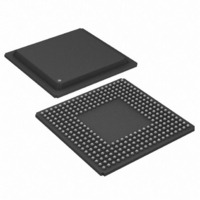
... TRANSMIT LINE INTERFACE SIDE AC TIMING Figure 24- TCLK TPOS, TNEG t DD 25. MCM PACKAGE DIMENSIONS DS21FF42 / DS21FT42 Mechanical Dimensions 113 of 114 ...
Page 114
POWER SUPPLY DE-COUPLING In a typical PCB layout for the MCM, all of the VDD pins will connect to a common power plane and all the VSS lines will connect to a common ground plane. The recommended method for de-coupling ...