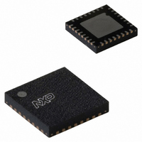
TDA8025HN/C1,557 NXP Semiconductors, TDA8025HN/C1,557 Datasheet - Page 11

TDA8025HN/C1,557
Manufacturer Part Number
TDA8025HN/C1,557
Description
IC SMART CARD INTERFACE 32-HVQFN
Manufacturer
NXP Semiconductors
Datasheet
1.TDA8025HNC1518.pdf
(38 pages)
Specifications of TDA8025HN/C1,557
Controller Type
Smart Card Interface
Interface
Analog
Voltage - Supply
1.2V, 1.8V, 3V
Current - Supply
65mA
Operating Temperature
-25°C ~ 85°C
Mounting Type
Surface Mount
Package / Case
32-VQFN Exposed Pad, 32-HVQFN, 32-SQFN, 32-DHVQFN
Lead Free Status / RoHS Status
Lead free / RoHS Compliant
Other names
935286389557
NXP Semiconductors
TDA8025_1
Product data sheet
8.3 Clock circuits
If we target 1 % accuracy resistors ( = 0.01) and R
Table 8 on page
Deactivation always occurs when
where
With the resulting values for R1
page
The clock signal (pin CLK) to the card is either generated by the clock signal input on pin
XTAL1 or from a crystal (f
voltage level applied to pin ENCLKIN defines which clock signal is used. When pin
ENCLKIN is HIGH, connect the external clock to pin XTAL1.
Driving pin ENCLKIN LOW causes the external crystal to generate frequency f
pins CLKDIV1 and CLKDIV2, the crystal frequency can be set to either f
or
The frequency change is synchronous and as such during transition, no pulse is shorter
than 45 % of the smallest period. In addition, only the first and last clock pulse around the
change have the correct width. When dynamically changing the frequency, the
modification is only effective after 10 periods of XTAL1.
R1
-------------- -
R2
R2
V
•
•
•
•
•
max
PORADJ
1
nom
nom
nom
8
R1
R2
V
V
occurs
max
f
th(min)
DD(INTF)deactmax
23) then V
=
xtal
nom
nom
=
=
---------------------------------------------- -
1
.
------------------------------
---------------- -
+
1 +
1
1 –
= 50.88 k
= 49.12 k
V
is the minimum falling external threshold voltage
-------------------------------------
R2
R1
+
th min
R
R1
-------------- -
R2
sum
nom
nom
DD(INTF)deactmax
23) and V
1
nom
nom
V
--------------------------------------- - 1
1 –
1 +
DD INTF actmin
is the maximum value of V
V
=
V
DD INTF deactmax
Rev. 01 — 6 April 2009
th max
------------------------------------------------------------------------------------------- -
xtal
1
DD(INTF)actmin
=
+
---------------- -
--------------------------------------------- -
V
1 +
1 –
26 MHz) connected between pins XTAL1 and XTAL2. The
nom
is 2.28 V.
DD INTF deactmax
, R2
V
–
th min
nom
V
--------------------------------------- - 1
= 2.64 V then
R
=
DD INTF actmin
sum
V
------------------ -
and ; V
V
th min
th max
max
DD(INTF)
th(min)
sum
–
= 100 k ; V
below which deactivation always
= 1.17 V (see
th(max)
TDA8025
© NXP B.V. 2009. All rights reserved.
Table 8 on
xtal
IC card interface
= 1.33 V (see
,
1
2
f
xtal
xtal
. Using
,
1
11 of 38
4
(10)
(11)
(12)
f
xtal
(9)


