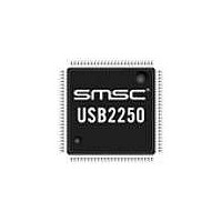
USB2250-NU-05 SMSC, USB2250-NU-05 Datasheet - Page 17

USB2250-NU-05
Manufacturer Part Number
USB2250-NU-05
Description
IC CTRLR USB2.0 FLASH 128VTQFP
Manufacturer
SMSC
Datasheet
1.USB2250-NU-05.pdf
(44 pages)
Specifications of USB2250-NU-05
Controller Type
FlashMedia Controller
Interface
Serial
Voltage - Supply
3 V ~ 3.6 V
Current - Supply
165mA
Operating Temperature
0°C ~ 70°C
Mounting Type
Surface Mount
Package / Case
128-TQFP, 128-VQFP
Operating Supply Voltage
3.3 V
Mounting Style
SMD/SMT
Operating Temperature Range
0 C to + 70 C
Supply Current
80 mA
Lead Free Status / Rohs Status
Lead free / RoHS Compliant
Other names
638-1088
Available stocks
Company
Part Number
Manufacturer
Quantity
Price
Company:
Part Number:
USB2250-NU-05
Manufacturer:
Intersil
Quantity:
171
Company:
Part Number:
USB2250-NU-05
Manufacturer:
Microchip Technology
Quantity:
10 000
Ultra Fast USB 2.0 Multi-Slot Flash Media Controller
Datasheet
SMSC USB2250/50i/51/51i
Memory
Data Bus
Memory
Address Bus
Memory Write
Strobe
Memory Read
Strobe
NAME
Table 6.1 USB2250/50i/51/51i 128-Pin VTQFP Pin Descriptions (continued)
SYMBOL
MA[15:2]
MA[1:0] /
SEL[1:0]
MD[7:0]
nMWR
nMRD
MA16
CLK_
128-PIN
VTQFP
MEMORY / IO INTERFACE
107
109
106
108
113
110
112
114
116
115
111
33
29
30
31
34
35
36
37
28
24
25
27
2
4
1
3
DATASHEET
BUFFER
I/O12PU
I/O12PD
17
TYPE
O12
O12
O12
O12
O12
These signals are used to transfer data
between the internal CPU and the external
program memory and have weak internal pull-
up resistors.
These signals address memory locations
within the external memory.
These signals address memory locations
within the external memory.
MA[1:0]: These signals address memory
locations within the external memory.
CLK_SEL[1:0]: During RESET_N assertion,
these pins will select the operating frequency
of the external clock, and the corresponding
weak pull-down resistors are enabled.
When RESET_N is negated, the value on
these pins will be latched internally and these
pins will revert to MA[1:0] functionality; the
internal pull-downs will be disabled.
CLK_SEL[1:0] = '00'. 24 MHz
CLK_SEL[1:0] = '01'. RESERVED
CLK_SEL[1:0] = '10'. RESERVED
CLK_SEL[1:0] = '11'. 48 MHz
If the latched value is '1', the corresponding
MA pin is tri-stated when the chip is in power
down state.
If the latched value is '0', the corresponding
MA pin will function identically to MA[15:3]
pins at all times (other than during RESET_N
assertion).
This pin is the active low program Memory
Write strobe signal.
This pin is the active low program Memory
Read strobe signal.
DESCRIPTION
Revision 2.0 (09-29-09)


