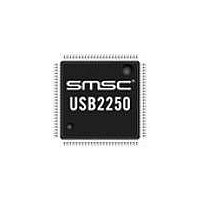
USB2250-NU-05 SMSC, USB2250-NU-05 Datasheet - Page 16

USB2250-NU-05
Manufacturer Part Number
USB2250-NU-05
Description
IC CTRLR USB2.0 FLASH 128VTQFP
Manufacturer
SMSC
Datasheet
1.USB2250-NU-05.pdf
(44 pages)
Specifications of USB2250-NU-05
Controller Type
FlashMedia Controller
Interface
Serial
Voltage - Supply
3 V ~ 3.6 V
Current - Supply
165mA
Operating Temperature
0°C ~ 70°C
Mounting Type
Surface Mount
Package / Case
128-TQFP, 128-VQFP
Operating Supply Voltage
3.3 V
Mounting Style
SMD/SMT
Operating Temperature Range
0 C to + 70 C
Supply Current
80 mA
Lead Free Status / Rohs Status
Lead free / RoHS Compliant
Other names
638-1088
Available stocks
Company
Part Number
Manufacturer
Quantity
Price
Company:
Part Number:
USB2250-NU-05
Manufacturer:
Intersil
Quantity:
171
Company:
Part Number:
USB2250-NU-05
Manufacturer:
Microchip Technology
Quantity:
10 000
Revision 2.0 (09-29-09)
SD Data 7-0
SD Clock
SD Command
SD Write
Protected GPIO
SD Card Detect
GPIO
USB Bus Data
USB Transceiver
Bias
24 MHz Crystal
Input (External
Clock Input)
24 MHz Crystal
Output
NAME
Table 6.1 USB2250/50i/51/51i 128-Pin VTQFP Pin Descriptions (continued)
SECURE DIGITAL (SD) / MULTIMEDIACARD (MMC) INTERFACE
SD_D[7:0]
(SD_nCD)
SYMBOL
SD_CMD
(SD_WP)
SD_CLK
GPIO15
(CLKIN)
GPIO6
RBIAS
XTAL1
XTAL2
USB+
USB-
128-PIN
VTQFP
105
127
124
123
13
11
19
21
22
23
10
12
18
20
32
7
8
USB INTERFACE
DATASHEET
BUFFER
I/O12PU
I/O12PU
OCLKx
16
TYPE
ICLKx
I/O12
I/O12
I/O-U
O12
I-R
These pins are bi-directional data signals
SD_D0 - SD_D7 and have weak pull-up
resistors.
This is an output clock signal to the SD/MMC
device.
The clock frequency is software configurable.
This is a bi-directional signal that connects to
the CMD signal of the SD/MMC device and
has a weak internal pull-up resistor.
This is a GPIO designated by the default
firmware as the Secure Digital card
mechanical write detect pin.
This is a GPIO designated by the default
firmware as the Secure Digital card detection
pin.
These pins connect to the USB bus data
signals.
A 12.0 kΩ, ±1.0% resistor is attached from
VSS to this pin in order to set the transceiver's
internal bias currents.
This pin can be connected to one terminal of
the crystal or it can be connected to an
external 24/48 MHz clock when a crystal is not
used.
The MA[1:0] pins will be sampled while
RESET_N is asserted, and the value will be
latched upon RESET_N negation. This will
determine the clock source and value.
This is the other terminal of the crystal, or it is
left open when an external clock source is
used to drive XTAL1(CLKIN). It may not be
used to drive any external circuitry other than
the crystal circuit.
Ultra Fast USB 2.0 Multi-Slot Flash Media Controller
DESCRIPTION
SMSC USB2250/50i/51/51i
Datasheet


