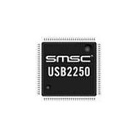
USB2250-NU-05 SMSC, USB2250-NU-05 Datasheet - Page 15

USB2250-NU-05
Manufacturer Part Number
USB2250-NU-05
Description
IC CTRLR USB2.0 FLASH 128VTQFP
Manufacturer
SMSC
Datasheet
1.USB2250-NU-05.pdf
(44 pages)
Specifications of USB2250-NU-05
Controller Type
FlashMedia Controller
Interface
Serial
Voltage - Supply
3 V ~ 3.6 V
Current - Supply
165mA
Operating Temperature
0°C ~ 70°C
Mounting Type
Surface Mount
Package / Case
128-TQFP, 128-VQFP
Operating Supply Voltage
3.3 V
Mounting Style
SMD/SMT
Operating Temperature Range
0 C to + 70 C
Supply Current
80 mA
Lead Free Status / Rohs Status
Lead free / RoHS Compliant
Other names
638-1088
Available stocks
Company
Part Number
Manufacturer
Quantity
Price
Company:
Part Number:
USB2250-NU-05
Manufacturer:
Intersil
Quantity:
171
Company:
Part Number:
USB2250-NU-05
Manufacturer:
Microchip Technology
Quantity:
10 000
Ultra Fast USB 2.0 Multi-Slot Flash Media Controller
Datasheet
SMSC USB2250/50i/51/51i
SM Chip Enable
SM Card
Detection GPIO
MS Bus State
MS Card
Insertion GPIO
MS System CLK
MS System Data
In/Out
MS System Data
In/Out
NAME
Table 6.1 USB2250/50i/51/51i 128-Pin VTQFP Pin Descriptions (continued)
(SM_nCD)
MS_SCLK
MS_D[7:1]
(MS_INS)
MS_SDIO
SYMBOL
SM_nCE
MS_D0 /
GPIO14
MS_BS
GPIO12
MEMORY STICK (MS) INTERFACE
128-PIN
VTQFP
101
100
54
57
91
98
97
93
95
99
96
92
94
DATASHEET
BUFFER
I/O12PD
I/O12PD
O12PU
15
TYPE
I/O12
O12
O12
IPU
This pin is the active low chip enable signal to
the SM device.
When using the internal FET, this pin has a
weak internal pull-up resistor that is tied to the
output of the internal power FET.
If an external FET is used (internal FET is
disabled), then the internal pull-up is not
available (external pull-ups must be used).
This is a GPIO designated by the default
firmware as the Smart Media card detection
pin.
This pin is connected to the bus state pin of
the MS device.
It is used to control the bus states 0, 1, 2 and
3 (BS0, BS1, BS2 and BS3) of the MS device.
This is a GPIO designated by the default
firmware as the Memory Stick card detection
pin.
This pin is an output clock signal to the MS
device. The clock frequency is software
configurable.
MS_D[7:1]: These pins are the bi-directional
data signals for the MS device.
MS_D2 and MS_D3 have weak pull-down
resistors. MS_D1 has a pull-down resistor if it
is in parallel mode, otherwise it is disabled.
In 4- or 8-bit parallel mode, each MS_D7:1
signal has a weak pull-down resistor.
MS_D0: This pin is one of the bi-directional
data signals for the MS device.
In serial mode, the most significant bit (MSB)
of each byte is transmitted first by either MSC
or the MS device on MS_D0, MS_D2, and
MS_D3 (which have weak pull-down
resistors). If MS_D1 is in parallel mode, it has
a pull-down resistor; Otherwise, it is disabled.
In 4- or 8-bit parallel mode, the MS_D0 signal
has a weak pull-down resistor.
MS_SDIO: Serial Data Bus. This pin is
responsible for transfer direction and types of
data change depending on the bus state.
DESCRIPTION
Revision 2.0 (09-29-09)


