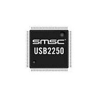
USB2250-NU-05 SMSC, USB2250-NU-05 Datasheet - Page 12

USB2250-NU-05
Manufacturer Part Number
USB2250-NU-05
Description
IC CTRLR USB2.0 FLASH 128VTQFP
Manufacturer
SMSC
Datasheet
1.USB2250-NU-05.pdf
(44 pages)
Specifications of USB2250-NU-05
Controller Type
FlashMedia Controller
Interface
Serial
Voltage - Supply
3 V ~ 3.6 V
Current - Supply
165mA
Operating Temperature
0°C ~ 70°C
Mounting Type
Surface Mount
Package / Case
128-TQFP, 128-VQFP
Operating Supply Voltage
3.3 V
Mounting Style
SMD/SMT
Operating Temperature Range
0 C to + 70 C
Supply Current
80 mA
Lead Free Status / Rohs Status
Lead free / RoHS Compliant
Other names
638-1088
Available stocks
Company
Part Number
Manufacturer
Quantity
Price
Company:
Part Number:
USB2250-NU-05
Manufacturer:
Intersil
Quantity:
171
Company:
Part Number:
USB2250-NU-05
Manufacturer:
Microchip Technology
Quantity:
10 000
Chapter 6 Pin Descriptions
Revision 2.0 (09-29-09)
6.1
CF Chip Select 0
CF Register
Address
CF Interrupt
CF Data 15-8 /
GPIO
NAME
This section provides a detailed description of each signal. The signals are arranged in functional
groups according to their associated interface. The pin descriptions are applied when using the internal
default firmware and can be referenced in
reference
The “n” symbol in the signal name indicates that the active, or asserted, state occurs when the signal
is at a low voltage level. When “n” is not present in the signal name, the signal is asserted at the high
voltage level.
The terms assertion and negation are used exclusively. This is done to avoid confusion when working
with a mixture of “active low” and “active high” signals. The term assert, or assertion, indicates that a
signal is active, independent of whether that level is represented by a high or low voltage. The term
negate, or negation, indicates that a signal is inactive.
128-Pin VTQFP Pin Descriptions
Table 6.1 USB2250/50i/51/51i 128-Pin VTQFP Pin Descriptions
CF_D[15:8] /
GPIO[31:24]
CF_SA[2:0]
Chapter 1, "Acronyms," on page 6
CF_nCS0
SYMBOL
CF_IRQ
COMPACT FLASH (CF) INTERFACE
128-PIN
VTQFP
71
82
83
84
74
70
68
66
62
60
90
89
87
DATASHEET
BUFFER
I/O12PD
O12PU
12
TYPE
I/O12
I/O12
IPD
Chapter 8, "Configuration Options," on page
for a list of the acronyms used.
This pin is the active low chip select 0 signal
for the task file registers of the CF ATA device
in True IDE mode. This pin has a weak
internal pull-up resistor.
These pins are the register select address bits
for the CF ATA device.
This is the active high interrupt request signal
from the CF device. This pin has a weak
internal pull-down resistor.
CF_D[15:8]: These pins are the bi-directional
data signals CF_D15 - CF_D8 in True IDE
mode data transfer.
In True IDE mode, all task file register
operations occur on CF_D[7:0], while data
transfer occurs on CF_D[15:0].
These bi-directional data signals have weak
internal pull-down resistors.
GPIO[31:24]: These pins may be used either
as input, edge sensitive interrupt input, or
output. Custom firmware is required to activate
this function.
Ultra Fast USB 2.0 Multi-Slot Flash Media Controller
DESCRIPTION
SMSC USB2250/50i/51/51i
24. Please
Datasheet


