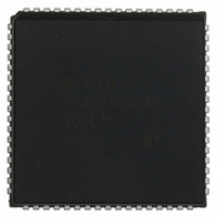
Z16C3220VSG Zilog, Z16C3220VSG Datasheet - Page 91

Z16C3220VSG
Manufacturer Part Number
Z16C3220VSG
Description
IC Z16C32 MCU 20MHZ IUSC 68PLCC
Manufacturer
Zilog
Series
IUSC™r
Specifications of Z16C3220VSG
Controller Type
USC Controller
Interface
DMA
Voltage - Supply
4.5 V ~ 5.5 V
Current - Supply
7mA
Operating Temperature
0°C ~ 70°C
Mounting Type
Surface Mount
Package / Case
68-LCC (J-Lead)
Lead Free Status / RoHS Status
Lead free / RoHS Compliant
Other names
269-4689-5
Z16C3220VSG
Z16C3220VSG
Available stocks
Company
Part Number
Manufacturer
Quantity
Price
Company:
Part Number:
Z16C3220VSG
Manufacturer:
Zilog
Quantity:
40
Company:
Part Number:
Z16C3220VSG
Manufacturer:
F
Quantity:
6 229
IUSC TIMING
The IUSC interface timing is similar to that found on a static
RAM, except that it is much more flexible. Up to four
separate timing strobe signals are present on the inter-
face: /DS, /RD, /WR and /INTACK. Only one of these timing
strobes is active at any time. Should the external logic
activate more than one of these strobes at the same time,
DC CHARACTERISTICS
Note:
V
AC CHARACTERISTICS
Timing Diagrams (Figures 83-105)
91
Z
ILOG
CC
Symbol
V
V
V
V
V
I
I
I
IL
OL
CC1
/RESET
IH
IL
OH1
OH2
OL
= 5V ± 10% unless otherwise specified, over specified temperature range.
/STB
/STB
Parameter
Input High Voltage
Input Low Voltage
Output High Voltage
Output High Voltage
Output Low Voltage
Input Leakage
Output Leakage
V
CC
Supply Current
Note:
/STB is any of the following: /DS, /RD, /WR or Pulsed /INTACK.
V
CC
–0.3
Min
2.2
2.4
Figure 84. Bus Cycle Timing
P R E L I M I N A R Y
–0.8
Figure 83. Reset Timing
Typ
7
the IUSC will enter a pre-reset state. This state is only
exited by a hardware reset. Do not allow overlap of timing
strobes. The timing diagrams, beginning on the next page,
illustrate the different bus transactions possible with the
necessary setup, hold, and delay times. IUSC Timing
diagrams are shown from Figure 83 through Figure 107.
V
+10.00
+10.00
CC
Max
0.8
0.4
50
+0.3
Unit
mA
μA
μA
V
V
V
V
V
Condition
I
I
I
0.4 < V
0.4 < V
V
OH
OH
OL
CC
= +2.0 mA
= –1.6 mA
= –250 μA
= 5V V
IN
OUT
< +2.4V
IH
< +2.4V
= 4.8V V
PS97USC0200
Z16C32 IUSC
IL
= 0.2V
™


