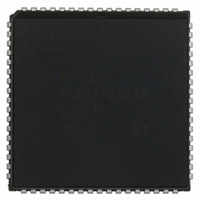
Z16C3220VSG Zilog, Z16C3220VSG Datasheet - Page 116

Z16C3220VSG
Manufacturer Part Number
Z16C3220VSG
Description
IC Z16C32 MCU 20MHZ IUSC 68PLCC
Manufacturer
Zilog
Series
IUSC™r
Specifications of Z16C3220VSG
Controller Type
USC Controller
Interface
DMA
Voltage - Supply
4.5 V ~ 5.5 V
Current - Supply
7mA
Operating Temperature
0°C ~ 70°C
Mounting Type
Surface Mount
Package / Case
68-LCC (J-Lead)
Lead Free Status / RoHS Status
Lead free / RoHS Compliant
Other names
269-4689-5
Z16C3220VSG
Z16C3220VSG
Available stocks
Company
Part Number
Manufacturer
Quantity
Price
Company:
Part Number:
Z16C3220VSG
Manufacturer:
Zilog
Quantity:
40
Company:
Part Number:
Z16C3220VSG
Manufacturer:
F
Quantity:
6 229
Notes:
AC Test Conditions:
V
V
V
Float = +0.5V
[1] Direct Address is any of S//D, D//C or AD15-AD8 used
[2] The parameter applies only when /AS is not present.
[3] Strobe is any of /DS, /RD, /WR or Pulsed /INTACK.
[4] Parameter applies only if read empties the receive FIFO.
[5] Parameter applies only if write fills the transmit FIFO.
[6] Parameter applies only while the IUSC is bus master.
Z
PS97USC0200
ILOG
CC
IH
IL
No
147
148
149
150
151
152
153
154
155
156
157
158
159
160
161
162
163
164
165
166
167
168
169
170
171
172
173
174
175
176
= 0.8V V
= 2.0V V
= 5V ± 5% unless otherwise specified,
as an address bus.
over specified temperature range.
OL
OH
= 0.8V
= 2.0V
Symbol
TdCLK(ADz)
TdCLK(ADa)
TsAD(UAS)
ThAD(UAS)
TsAD(AS)
ThAD(AS)
TsW(CLK)
ThW(CLK)
TsRDY(CLK)
ThRDY(CLK)
ThDW(CLK)
TdAS(DSw)
TsDW(DS)
TwDSlw
ThDW(DS)
TdAS(WR)
TsDW(WR)
TwWRl
ThDW(WR)
TdCLK(WR)
TdCLK(BUSz)
TsABT(CLK)
ThABT(CLK)
TdCLK(BRQ)
TdCLK(BUSa)
TsBIN(CLK)
ThBIN(CLK)
TsBRQ(CLK)
ThBRQ(CLK)
TdBIN(BOT)
Parameter
CLK Rise to Address Float Delay
CLK Rise to Address Active Delay
Address to /UAS Rise Setup Time
Address to /UAS Rise Hold Time
Address to /AS Rise Setup Time
Address to /AS Rise Hold Time
/WAIT to CLK Fall Setup Time
/WAIT to CLK Fall Hold Time
/READY to CLK Fall Setup Time
/READY to CLK Fall Hold Time
Write Data to CLK Rise Hold Time
/AS Rise to /DS Fall (Write) Delay
Write Data to /DS Fall Setup Time
/DS (Write) Low Width
Write Data to /DS Rise Hold Time
/AS Rise to /WR Fall Delay
Write Data to /WR Fall Setup Time
/WR Low Width
Write Data to /WR Rise Hold Time
CLK Fall to /WR Delay
CLK Rise to Bus Float Delay
/ABORT to CLK Rise Setup Time
/ABORT to CLK Rise Hold Time
CLK Rise to /BUSREQ Delay
CLK Rise to Bus Active Delay
/BIN to CLK Rise Setup Time
/BIN to CLK Rise Hold Time
/BUSREQ to CLK Rise Setup Time
/BUSREQ to CLK Rise Hold Time
/BIN to /BOUT Delay
P R E L I M I N A R Y
[7] Parameter is clock-cycle dependent, TwCLKh + TfCLK – 5.
[8] Parameter is clock-cycle dependent, TwCLKl + TrCLK –5
[9] Parameter is clock-cycle dependent,
[10] Parameter is clock-cycle dependent, TcCLK –10.
[11] Parameter is clock-cycle dependent, TcCLK –5.
[12] Clock cycle parameters TwCLKh and TcCLK have unique
[13] For Linked List Mode, the minimum for these values should be
TcCLK + TwCLKh + TfCLK –5.
values for Linked List Mode. In Linked List Mode, the system clock
cycle is extended to 60 ns, and the system clock High pulse width
is extended to 35 ns. This is due to the internal timing paths unique
to the Linked List Mode. The transmit and receive bit rates are not
affected.
calculated using TwCLKh = 35 ns and TcCLK = 60 ns.
Min
10
10
10
10
10
15
10
15
40
25
45
25
40
25
45
25
20
15
20
15
25
0
0
Max
35
35
30
30
30
30
60
Units
ns
ns
ns
ns
ns
ns
ns
ns
ns
ns
ns
ns
ns
ns
ns
ns
ns
ns
ns
ns
ns
ns
ns
ns
ns
ns
ns
ns
ns
ns
Z16C32 IUSC
[6,10,13]
[6,11,13]
[6,10,13]
[6,11,13]
[6,7,13]
[6,7,13]
Note
[6,8]
[6,8]
[6]
[6]
[6]
[6]
[6]
[6]
[6]
[6]
[6]
[6]
[6]
[6]
[6]
[6]
[6]
[6]
[6]
[6]
[6]
[6]
[6]
116
™


