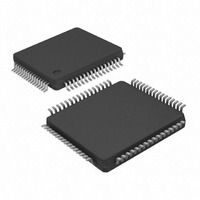
KSZ8873MLL Micrel Inc, KSZ8873MLL Datasheet - Page 39

KSZ8873MLL
Manufacturer Part Number
KSZ8873MLL
Description
IC ETHERNET SWITCH 3PORT 64-LQFP
Manufacturer
Micrel Inc
Specifications of KSZ8873MLL
Data Rate
100Mbps
Controller Type
Ethernet Switch Controller
Interface
MII
Voltage - Supply
1.8V, 2.5V, 3.3V
Operating Temperature
0°C ~ 70°C
Mounting Type
Surface Mount
Package / Case
64-LQFP
No. Of Ports
3
Ethernet Type
IEEE 802.3u
Supply Current
115mA
Supply Voltage Range
2.5V, 3.3V
Digital Ic Case Style
LQFP
No. Of Pins
64
Svhc
No SVHC (15-Dec-2010)
Base
RoHS Compliant
Number Of Primary Switch Ports
3
Internal Memory Buffer Size
32
Fiber Support
No
Integrated Led Drivers
Yes
Phy/transceiver Interface
MII
Power Supply Type
Analog/Digital
Data Rate (typ)
10/100Mbps
Vlan Support
Yes
Operating Temperature (max)
70C
Operating Temperature (min)
0C
Mounting
Surface Mount
Jtag Support
No
Operating Supply Voltage (max)
1.89/3.465V
Operating Temperature Classification
Commercial
Interface Type
MII, RMII
Operating Temperature Range
0°C To +70°C
Rohs Compliant
Yes
Lead Free Status / RoHS Status
Lead free / RoHS Compliant
Current - Supply
-
Lead Free Status / RoHS Status
Compliant, Lead free / RoHS Compliant
Other names
576-3459
Available stocks
Company
Part Number
Manufacturer
Quantity
Price
Company:
Part Number:
KSZ8873MLL
Manufacturer:
Micrel Inc
Quantity:
1 934
Company:
Part Number:
KSZ8873MLL
Manufacturer:
ADI
Quantity:
27
Company:
Part Number:
KSZ8873MLL AM
Manufacturer:
Micrel
Quantity:
1 638
Company:
Part Number:
KSZ8873MLLJ
Manufacturer:
Micrel
Quantity:
323
Micrel, Inc.
SPI Slave Serial Bus Configuration
In managed mode, the KSZ8873MLL/FLL/RLL can be configured as a SPI slave device. In this mode, a SPI master
device (external controller/CPU) has complete programming access to the KSZ8873MLL/FLL/RLL’s 198 registers.
Programming access includes the Global Registers, Port Registers, Advanced Control Registers and indirect access to
the “Static MAC Table”, “VLAN Table”, “Dynamic MAC Table” and “MIB Counters”. The tables and counters are indirectly
accessed via registers 121 to 131.
The KSZ8873MLL/FLL/RLL supports two standard SPI commands: ‘0000_0011’ for data read and ‘0000_0010’ for data
write. SPI multiple read and multiple write are also supported by the KSZ8873MLL/FLL/RLL to expedite register read back
and register configuration, respectively.
SPI multiple read is initiated when the master device continues to drive the KSZ8873MLL/FLL/RLL SPISN input pin (SPI
Slave Select signal) low after a byte (a register) is read. The KSZ8873MLL/FLL/RLL internal address counter increments
automatically to the next byte (next register) after the read. The next byte at the next register address is shifted out onto
the KSZ8873MLL/FLL/RLL SPIQ output pin. SPI multiple read continues until the SPI master device terminates it by de-
asserting the SPISN signal to the KSZ8873MLL/FLL/RLL.
Similarly, SPI multiple write is initiated when the master device continues to drive the KSZ8873MLL/FLL/RLL SPISN input
pin low after a byte (a register) is written. The KSZ8873MLL/FLL/RLL internal address counter increments automatically to
the next byte (next register) after the write. The next byte that is sent from the master device to the KSZ8873MLL/FLL/RLL
SDA input pin is written to the next register address. SPI multiple write continues until the SPI master device terminates it
by de-asserting the SPISN signal to the KSZ8873MLL/FLL/RLL.
For both SPI multiple read and multiple write, the KSZ8873MLL/FLL/RLL internal address counter wraps back to register
address zero once the highest register address is reached. This feature allows all 198 KSZ8873MLL/FLL/RLL registers to
be read, or written with a single SPI command from any initial register address.
The KSZ8873MLL/FLL/RLL is capable of supporting a SPI bus.
The following is a sample procedure for programming the KSZ8873MLL/FLL/RLL using the SPI bus:
1. At the board level, connect the KSZ8873MLL/FLL/RLL pins as follows:
2. Enable SPI slave mode by setting the KSZ8873MLL/FLL/RLL strap-in pins P2LED[1:0] to “10”.
3. Power up the board and assert reset to the KSZ8873MLL/FLL/RLL.
4. Configure the desired register settings in the KSZ8873MLL/FLL/RLL, using the SPI write or multiple write command.
5. Read back and verify the register settings in the KSZ8873MLL/FLL/RLL, using the SPI read or multiple read
Some of the configuration settings, such as “Aging enable”, “Auto Negotiation Enable”, “Force Speed” and “Power down” can
be programmed after the switch has been started.
The following four figures illustrate the SPI data cycles for “Write”, “Read”, “Multiple Write” and “Multiple Read”. The read data is
registered out of SPIQ on the falling edge of SPIC, and the data input on SPID is registered on the rising edge of SPIC.
September 2010
command.
KSZ8873MLL/FLL/RLL Pin #
40
42
43
39
KSZ8873MLL/FLL/RLL Signal Name
SPISN
SCL
(SPIC)
SDA
(SPID)
SPIQ
Table 13. SPI Connections
39
External Processor Signal Description
SPI Slave Select
SPI Clock
SPI Data
(Master output; Slave input)
SPI Data
(Master input; Slave output)
KSZ8873MLL/FLL/RLL
M9999-092309-1.2


