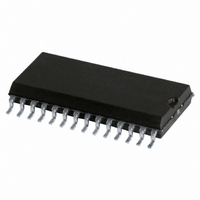
SJA1000T/N1,112 NXP Semiconductors, SJA1000T/N1,112 Datasheet - Page 55

SJA1000T/N1,112
Manufacturer Part Number
SJA1000T/N1,112
Description
IC STAND-ALONE CAN CTRLR 28-SOIC
Manufacturer
NXP Semiconductors
Datasheet
1.SJA1000TN1112.pdf
(68 pages)
Specifications of SJA1000T/N1,112
Package / Case
28-SOIC (7.5mm Width)
Controller Type
CAN Interface
Interface
CAN
Voltage - Supply
4.5 V ~ 5.5 V
Current - Supply
15mA
Operating Temperature
-40°C ~ 125°C
Mounting Type
Surface Mount
Product
Controller Area Network (CAN)
Number Of Transceivers
1
Data Rate
1 Mbps
Supply Voltage (max)
5.5 V
Supply Voltage (min)
4.5 V
Supply Current (max)
15 mA
Maximum Operating Temperature
+ 125 C
Minimum Operating Temperature
- 40 C
Mounting Style
SMD/SMT
Lead Free Status / RoHS Status
Lead free / RoHS Compliant
Lead Free Status / RoHS Status
Lead free / RoHS Compliant, Lead free / RoHS Compliant
Other names
568-3994-5
935230920112
SJA1000TD
SJA1000TD
935230920112
SJA1000TD
SJA1000TD
Philips Semiconductors
Table 48 Output pin configuration; note 1
Notes
1. X = don’t care.
2. TPX is the on-chip output transistor X, connected to V
3. TNX is the on-chip output transistor X, connected to V
4. TXX is the serial output level on pin TX0 or TX1. It is required that the output level on the CAN-bus line is dominant
The bit sequence (TXD) is sent via TX0 and TX1.
The voltage levels on the output driver pins depends on
both the driver characteristics programmed by OCTP,
OCTN (float, pull-up, pull-down, push-pull) and the output
polarity programmed by OCPOL.
6.5.4
The clock divider register controls the CLKOUT frequency
for the microcontroller and allows to deactivate the
CLKOUT pin. Additionally a dedicated receive interrupt
pulse on TX1, a receive comparator bypass and the
Table 49 Bit interpretation of the clock divider register (CDR); CAN address 31
Note
1. This bit cannot be written. During read-out of this register always a zero is given.
2000 Jan 04
Float
Pull-down
Pull-up
Push-pull
CAN mode
Stand-alone CAN controller
DRIVE
when TXD = 0 and recessive when TXD = 1.
BIT 7
C
LOCK
D
IVIDER
BIT 6
TXD
CBP
X
0
1
0
1
0
1
0
1
0
1
0
1
R
EGISTER
RXINTEN
OCTPX
BIT 5
(CDR)
0
0
0
0
0
1
1
1
1
1
1
1
1
OCTNX
BIT 4
(0)
0
1
1
1
1
0
0
0
0
1
1
1
1
(1)
DD
SS
55
.
.
selection between BasicCAN mode and PeliCAN mode is
made here. The default state of the register after hardware
reset is divide-by-12 for Motorola mode (00000101) and
divide-by-2 for Intel mode (00000000).
On software reset (reset request/reset mode) this register
is not influenced.
The reserved bit (CDR.4) will always reflect a logic 0.
The application software should always write a logic 0 to
this bit in order to be compatible with future features, which
may be 1-active using this bit.
OCPOLX
clock off
BIT 3
X
0
0
1
1
0
0
1
1
0
0
1
1
TPX
BIT 2
CD.2
off
off
off
off
off
off
on
on
off
off
on
on
off
(2)
TNX
BIT 1
CD.1
off
on
off
off
on
off
off
off
off
on
off
off
on
(3)
Product specification
SJA1000
TXX
HIGH
HIGH
HIGH
HIGH
BIT 0
LOW
LOW
LOW
LOW
CD.0
float
float
float
float
float
(4)


