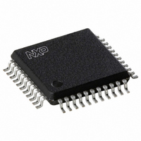
UDA1384H/N1,557 NXP Semiconductors, UDA1384H/N1,557 Datasheet - Page 21

UDA1384H/N1,557
Manufacturer Part Number
UDA1384H/N1,557
Description
IC AUDIO CODEC 44-QFP
Manufacturer
NXP Semiconductors
Type
Audio Codecr
Datasheet
1.UDA1384HN1557.pdf
(55 pages)
Specifications of UDA1384H/N1,557
Data Interface
I²C, Serial
Resolution (bits)
24 b
Number Of Adcs / Dacs
5 / 6
Sigma Delta
No
S/n Ratio, Adcs / Dacs (db) Typ
98 / 110 (Differential), 98 / 110 (Single-Ended)
Voltage - Supply, Analog
2.7 V ~ 3.6 V
Voltage - Supply, Digital
2.7 V ~ 3.6 V
Operating Temperature
-20°C ~ 85°C
Mounting Type
Surface Mount
Package / Case
44-MQFP, 44-PQFP
Lead Free Status / RoHS Status
Lead free / RoHS Compliant
Other names
568-3450
935274756557
UDA1384H
935274756557
UDA1384H
Available stocks
Company
Part Number
Manufacturer
Quantity
Price
Company:
Part Number:
UDA1384H/N1,557
Manufacturer:
NXP Semiconductors
Quantity:
10 000
Philips Semiconductors
9397 750 14366
Product data sheet
10.10 Write and read data
10.8 Device address
10.9 Register address
A slave receiver which is addressed, must generate an acknowledge after the reception of
each byte. Also a master must generate an acknowledge after the reception of each byte
that has been clocked out of the slave transmitter.
The device that acknowledges has to pull down the SDA line during the acknowledge
clock pulse, so the SDA line is stable LOW during the HIGH period of the acknowledge
related clock pulse. Set-up and hold times must be taken into account. A master receiver
must signal an end of data to the transmitter by not generating an acknowledge on the last
byte that has been clocked out of the slave. In this event, the transmitter must leave the
data line HIGH to enable the master to generate a stop condition.
Before any data is transmitted on the I
addressed first. The addressing is always done with byte 1 transmitted after the start
procedure. The UDA1384 acts as a slave receiver or a slave transmitter.
Therefore, the clock signal SCL is only an input signal. The data signal SDA is a
bidirectional line. The UDA1384 device address is shown in
Table 17:
The register addresses in the I
register addresses are defined in
The I
respectively.
Device address
Fig 15. Acknowledge on the I
A6
0
2
C-bus configurations for a write and read cycle are shown in
by transmitter
data output
by receiver
data output
SCL from
I
2
master
C-bus device address of UDA1384
A5
0
condition
START
Rev. 02 — 17 January 2005
S
A4
1
2
C-bus
2
C-bus mode are the same as in the L3-bus mode. The
Section
1
A3
2
1
C-bus, the device which should respond is
11.
2
A2
0
Multichannel audio coder-decoder
© Koninklijke Philips Electronics N.V. 2005. All rights reserved.
not acknowledge
Table
A1
0
acknowledge
8
17.
Table 18
acknowledgement
clock pulse for
UDA1384
A0
0
9
and
mbc602
R/W
Table
0/1
21 of 55
19,


