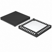
MAX9856ETL+T Maxim Integrated Products, MAX9856ETL+T Datasheet - Page 25

MAX9856ETL+T
Manufacturer Part Number
MAX9856ETL+T
Description
IC AUDIO CODEC 40TQFN-EP
Manufacturer
Maxim Integrated Products
Type
Audio Codecr
Datasheet
1.MAX9856ETL.pdf
(46 pages)
Specifications of MAX9856ETL+T
Data Interface
Serial
Resolution (bits)
18 b
Number Of Adcs / Dacs
2 / 2
Sigma Delta
Yes
S/n Ratio, Adcs / Dacs (db) Typ
77 / 91
Dynamic Range, Adcs / Dacs (db) Typ
85 / 91
Voltage - Supply, Analog
1.71 V ~ 3.6 V
Voltage - Supply, Digital
1.71 V ~ 3.6 V
Operating Temperature
-40°C ~ 85°C
Mounting Type
Surface Mount
Package / Case
40-WFQFN Exposed Pad
Lead Free Status / RoHS Status
Lead free / RoHS Compliant
The stereo ADC is capable of outputting data at any
sample rate from 8kHz to 48kHz. Data can be output in
common formats including left justified, I
(Figure 1). Figure 2 shows the digital timing in both
slave and master modes.
Figure 2. Digital Audio Interface Timing Diagrams
Table 7. ADC Interface Registers
ADC Interface Register Bit Description
SDIN/LRCLK (INPUTS)
BCLK (BCI = 0, INPUT)
BCLK (BCI = 1, INPUT)
0x0A
REG
0x07
0x08
0x09
SDOUT (OUTPUT)
DAI STEREO SERIAL INTERFACE TIMING DIAGRAM (SLAVE MODE)
REGISTER
AWCI
ABCI
______________________________________________________________________________________
APLLEN
AWCI
t SU
B7
t r, t f
ADC Word Clock (LRCLK_A) Invert
When PCM = 0:
0—Left-channel data is transmitted while LRCLK_A is low.
1—Right-channel data is transmitted while LRCLK_A is low.
When PCM = 1:
0—Start of a new frame is signified by the falling edge of the LRCLK_A pulse.
1—Start of a new frame is signified by the rising edge of the LRCLK_A pulse.
ADC BCLK Invert:
0—SDOUT is valid on the rising edge of BCLK.
1—SDOUT is valid on the falling edge of BCLK.
If operating in master mode, the ABCI bit has no effect. The DBCI bit controls BCLK to LRCLK_A
timing.
t DLY
t HD
ABCI
DirectDrive Headphone Amplifiers
B6
t BCLKS
ADC Interface
AGAIN
t BCLKH, t BCLKL
2
Low-Power Audio CODEC with
S, and PCM
B5
APIN
B4
If the DAC and ADC operate at the same sample rate
only the LRCLK_D is needed, allowing the LRCLK_A
pin to be reassigned as a GPIO. When configured as a
general-purpose output, LRCLK_A can be set high or
low by the APIN bits. When configured as a general-
purpose input, the status is reported in register 0x00.
Table 7 lists and describes the ADC interface registers.
ADCNI[7:0]
SDOUT/LRCLK (OUTPUTS)
DAI STEREO SERIAL INTERFACE TIMING DIAGRAM (MASTER MODE)
BCLK (OUTPUT)
SDIN (INPUT)
FUNCTION
ADCNI[14:8]
ADLY
B3
t SU
t r, t f
B2
0
t DLY
t HD
ANTH
t BCLKM
t BCLKH, t BCLKL
B1
0
B0
0
25


