MPC8313EVRAFFB Freescale Semiconductor, MPC8313EVRAFFB Datasheet - Page 91
MPC8313EVRAFFB
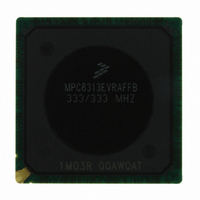
Manufacturer Part Number
MPC8313EVRAFFB
Description
IC MPU POWERQUICC II PRO 516PBGA
Manufacturer
Freescale Semiconductor
Datasheet
1.MPC8313CZQAFFB.pdf
(100 pages)
Specifications of MPC8313EVRAFFB
Processor Type
MPC83xx PowerQUICC II Pro 32-Bit
Speed
333MHz
Voltage
0.95 V ~ 1.05 V
Mounting Type
Surface Mount
Package / Case
516-PBGA
Processor Series
MPC8xxx
Core
e300
Data Bus Width
32 bit
Development Tools By Supplier
MPC8313E-RDB
Maximum Clock Frequency
400 MHz
Operating Supply Voltage
- 0.3 V to + 1.26 V
Maximum Operating Temperature
+ 105 C
Mounting Style
SMD/SMT
Data Ram Size
16 KB
I/o Voltage
2.5 V
Interface Type
I2C, SPI, UART
Minimum Operating Temperature
- 40 C
Program Memory Type
EEPROM/Flash
For Use With
MPC8313E-RDB - BOARD PROCESSOR
Lead Free Status / RoHS Status
Lead free / RoHS Compliant
Features
-
Lead Free Status / Rohs Status
Lead free / RoHS Compliant
Available stocks
Company
Part Number
Manufacturer
Quantity
Price
Company:

Part Number:
MPC8313EVRAFFB
Manufacturer:
FREESCAL
Quantity:
150
Company:
Part Number:
MPC8313EVRAFFB
Manufacturer:
Freescale Semiconductor
Quantity:
10 000


The value of this resistance and the strength of the driver’s current source can be found by making two
measurements. First, the output voltage is measured while driving logic 1 without an external differential
termination resistor. The measured voltage is V
while driving logic 1 with an external precision differential termination resistor of value R
measured voltage is V
R
Table 72
nominal NV
22.7
The MPC8313E provides the user with power-on configuration options which can be set through the use
of external pull-up or pull-down resistors of 4.7 kΩ on certain output pins (see customer visible
configuration pins). These pins are generally used as output only pins in normal operation.
While HRESET is asserted however, these pins are treated as inputs. The value presented on these pins
while HRESET is asserted, is latched when PORESET deasserts, at which time the input receiver is
disabled and the I/O circuit takes on its normal function. Careful board layout with stubless connections
to these pull-up/pull-down resistors coupled with the large value of the pull-up/pull-down resistor should
minimize the disruption of signal quality or speed for output pins thus configured.
Freescale Semiconductor
Note: Nominal supply voltages. See
term
Impedance
Differential
R
R
× (V
N
P
summarizes the signal impedance targets. The driver impedance are targeted at minimum V
Configuration Pin Muxing
1
/V
DD
2
, 105°C.
– 1). The drive current is then I
Configuration, Power
Local Bus, Ethernet,
DUART, Control,
MPC8313E PowerQUICC
Management
42 Target
42 Target
2
= (1/(1/R
NA
Table
Figure 60. Driver Impedance Measurement
1
Data
+ 1/R
Table 72. Impedance Characteristics
1, T
(Not Including PCI
J
Output Clocks)
2
= 105°C.
™
)) × I
PCI Signals
II Pro Processor Hardware Specifications, Rev. 3
25 Target
25 Target
NA
1
source
source
= R
source
. Solving for the output impedance gives R
= V
1
× I
PCI Output Clocks
/R
PCI_SYNC_OUT)
Pad
source
R
source
R
NV
(Including
N
P
42 Target
42 Target
V
SS
DD
NA
. Second, the output voltage is measured
.
SW2
SW1
DDR DRAM
20 Target
20 Target
NA
System Design Information
Symbol
Z
term
DIFF
Z
Z
0
0
. The
source
Unit
=
Ω
Ω
Ω
DD
91
,
Related parts for MPC8313EVRAFFB
Image
Part Number
Description
Manufacturer
Datasheet
Request
R

Part Number:
Description:
Mpc8313e Powerquicc Ii Pro Processor
Manufacturer:
Freescale Semiconductor, Inc
Datasheet:

Part Number:
Description:
BOARD PROCESSOR
Manufacturer:
Freescale Semiconductor
Datasheet:

Part Number:
Description:
BOARD CPU 8313E VER 2.1
Manufacturer:
Freescale Semiconductor
Datasheet:

Part Number:
Description:
BOARD CPU 8313E VER 2.2
Manufacturer:
Freescale Semiconductor
Datasheet:
Part Number:
Description:
Microprocessors - MPU 8313 REV2.2 PB ENC EXT
Manufacturer:
Freescale Semiconductor
Datasheet:
Part Number:
Description:
Microprocessors - MPU 8313 REV2.2 PB W/ENC
Manufacturer:
Freescale Semiconductor
Datasheet:
Part Number:
Description:
Manufacturer:
Freescale Semiconductor, Inc
Datasheet:
Part Number:
Description:
Manufacturer:
Freescale Semiconductor, Inc
Datasheet:
Part Number:
Description:
Manufacturer:
Freescale Semiconductor, Inc
Datasheet:
Part Number:
Description:
Manufacturer:
Freescale Semiconductor, Inc
Datasheet:
Part Number:
Description:
Manufacturer:
Freescale Semiconductor, Inc
Datasheet:
Part Number:
Description:
Manufacturer:
Freescale Semiconductor, Inc
Datasheet:
Part Number:
Description:
Manufacturer:
Freescale Semiconductor, Inc
Datasheet:
Part Number:
Description:
Manufacturer:
Freescale Semiconductor, Inc
Datasheet:
Part Number:
Description:
Manufacturer:
Freescale Semiconductor, Inc
Datasheet: