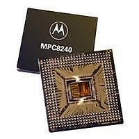
XPC8240LZU200E Freescale Semiconductor, XPC8240LZU200E Datasheet - Page 25

XPC8240LZU200E
Manufacturer Part Number
XPC8240LZU200E
Description
MCU HOST PROCESSOR 352-TBGA
Manufacturer
Freescale Semiconductor
Series
PowerQUICC IIr
Specifications of XPC8240LZU200E
Processor Type
MPC82xx PowerQUICC II 32-bit
Speed
200MHz
Voltage
2.5V
Mounting Type
Surface Mount
Package / Case
352-TBGA
Core Size
32 Bit
Program Memory Size
32KB
Cpu Speed
200MHz
Embedded Interface Type
I2C
Digital Ic Case Style
TBGA
No. Of Pins
352
Supply Voltage Range
2.5V To 2.75V
Rohs Compliant
No
Lead Free Status / RoHS Status
Contains lead / RoHS non-compliant
Features
-
Available stocks
Company
Part Number
Manufacturer
Quantity
Price
Company:
Part Number:
XPC8240LZU200E
Manufacturer:
MOTOLOLA
Quantity:
319
Company:
Part Number:
XPC8240LZU200E
Manufacturer:
Freescale Semiconductor
Quantity:
10 000
Part Number:
XPC8240LZU200E
Manufacturer:
FREESCALE
Quantity:
20 000
1.4.2.7
Table 15 provides the JTAG AC timing specifications for the MPC8240 while in the JTAG operating mode.
Figure 19 shows the JTAG clock input timing diagram.
MPC8240 Integrated Processor Hardware Specifications
At recommended operating conditions (see Table 2) with LV
Notes:
1. TRST is an asynchronous signal. The setup time is for test purposes only.
2. Non-test (other than TDI and TMS) signal input timing with respect to TCK.
3. Non-test (other than TDO) signal output timing with respect to TCK.
4. Timings are independent of the system clock (PCI_SYNC_IN).
Num
10
12
13
11
1
2
3
4
5
6
7
8
9
TCK frequency of operation
TCK cycle time
TCK clock pulse width measured at 1.5 V
TCK rise and fall times
TRST setup time to TCK falling edge
TRST assert time
Input data setup time
Input data hold time
TCK to output data valid
TCK to output high impedance
TMS, TDI data setup time
TMS, TDI data hold time
TCK to TDO data valid
TCK to TDO high impedance
IEEE 1149.1 (JTAG) AC Timing Specifications
Table 15. JTAG AC Timing Specification (Independent of PCI_SYNC_IN)
TCK
3
Characteristic
Freescale Semiconductor, Inc.
Figure 19. JTAG Clock Input Timing Diagram
For More Information On This Product,
Go to: www.freescale.com
VM = Midpoint Voltage
4
3
DD
VM
= 3.3 V ± 0.3 V
2
1
Electrical and Thermal Characteristics
Min
40
20
10
10
15
15
VM
0
0
5
0
0
5
0
0
2
Max
25
30
30
15
15
—
—
—
—
—
—
—
—
3
VM
MHz
Unit
ns
ns
ns
ns
ns
ns
ns
ns
ns
ns
ns
ns
ns
Notes
1
2
2
3
3
25


