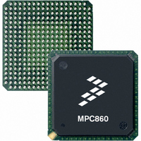
MPC855TZQ80D4 Freescale Semiconductor, MPC855TZQ80D4 Datasheet - Page 32

MPC855TZQ80D4
Manufacturer Part Number
MPC855TZQ80D4
Description
IC MPU POWERQUICC 80MHZ 357PBGA
Manufacturer
Freescale Semiconductor
Series
PowerQUICCr
Specifications of MPC855TZQ80D4
Processor Type
MPC8xx PowerQUICC 32-Bit
Speed
80MHz
Voltage
3.3V
Mounting Type
Surface Mount
Package / Case
357-PBGA
Processor Series
MPC8xx
Core
MPC8xx
Data Bus Width
32 bit
Maximum Clock Frequency
80 MHz
Operating Supply Voltage
2.5 V, 3.3 V
Maximum Operating Temperature
+ 95 C
Mounting Style
SMD/SMT
Minimum Operating Temperature
0 C
Core Size
32 Bit
Program Memory Size
8KB
Cpu Speed
80MHz
Digital Ic Case Style
BGA
No. Of Pins
357
Supply Voltage Range
3.135V To 3.465V
Rohs Compliant
No
Features
-
Lead Free Status / Rohs Status
Lead free / RoHS Compliant
Available stocks
Company
Part Number
Manufacturer
Quantity
Price
Company:
Part Number:
MPC855TZQ80D4
Manufacturer:
Freescale Semiconductor
Quantity:
10 000
Part Number:
MPC855TZQ80D4
Manufacturer:
FREESCALE
Quantity:
20 000
Ethernet: Three-Speed, MII Management
8.3.2
Table 28
32
At recommended operating conditions with LV
Input high current
Input low current
Note:
1. Note that the symbol V
MDC frequency
MDC period
MDC clock pulse width high
MDC to MDIO valid
MDC to MDIO delay
MDIO to MDC setup time
MDIO to MDC hold time
MDC rise time
MDC fall time
Notes:
1. The symbols used for timing specifications herein follow the pattern of t
2. This parameter is dependent on the system clock speed (that is, for a system clock of 267 MHz, the delay is 70 ns and for
3. This parameter is dependent on the CCB clock speed (that is, for a CCB clock of 267 MHz, the delay is 60 ns and for a
4. Guaranteed by design.
(reference)(state)
symbolizes management data timing (MD) for the time t
invalid (X) or data hold time. Also, t
signals (D) reach the valid state (V) relative to the t
rise and fall times, the latter convention is used with the appropriate letter: R (rise) or F (fall).
a system clock of 333 MHz, the delay is 58 ns).
CCB clock of 333 MHz, the delay is 48 ns).
Parameter/Condition
MPC8555E PowerQUICC™ III Integrated Communications Processor Hardware Specification, Rev. 4.2
Parameter
provides the MII management AC timing specifications.
MII Management AC Electrical Specifications
for inputs and t
Table 27. MII Management DC Electrical Characteristics (continued)
IN
, in this case, represents the OV
Table 28. MII Management AC Timing Specifications
(first two letters of functional block)(reference)(state)(signal)(state)
Symbol
I
I
IH
IL
MDDVKH
DD
Symbol
t
t
t
t
MDKHDX
MDDXKH
MDKHDV
MDDVKH
t
t
t
MDCH
MDCR
is 3.3 V ± 5%.
f
t
MDHF
MDC
MDC
LV
LV
symbolizes management data timing (MD) with respect to the time data input
DD
DD
1
= Max
= Max
MDC
Conditions
0.893
Min
MDC
clock reference (K) going to the high (H) state or setup time. For
96
32
10
IN
—
—
5
0
symbol referenced in
V
from clock reference (K) high (H) until data outputs (D) are
V
IN
IN
1
= 0.5 V
= 2.1 V
Typ
(first two letters of functional block)(signal)(state)
—
—
—
—
—
—
—
—
Table 1
–600
2*[1/(f
2*[1/(f
Min
for outputs. For example, t
—
1120
Max
10.4
and
ccb_clk
ccb_clk
10
10
—
—
—
Table
/8)]
/8)]
Freescale Semiconductor
2.
Max
40
—
MHz
Unit
ns
ns
ns
ns
ns
ns
ns
ns
MDKHDX
Notes
Unit
μA
μA
2
3
3


