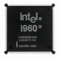
KU80960CA25 Intel, KU80960CA25 Datasheet - Page 9

KU80960CA25
Manufacturer Part Number
KU80960CA25
Description
IC MPU I960CA 5V 25MHZ 196QFP
Manufacturer
Intel
Datasheet
1.KU80960CA25.pdf
(68 pages)
Specifications of KU80960CA25
Rohs Status
RoHS non-compliant
Processor Type
i960
Features
CA suffix, 32-Bit with DMA
Speed
25MHz
Voltage
5V
Mounting Type
Surface Mount
Package / Case
196-QFP
Family Name
i960
Device Core Size
32b
Frequency (max)
25MHz
Instruction Set Architecture
RISC
Supply Voltage 1 (typ)
5V
Operating Supply Voltage (max)
5.5V
Operating Supply Voltage (min)
4.5V
Operating Temp Range
0C to 100C
Operating Temperature Classification
Commercial
Mounting
Surface Mount
Pin Count
196
Package Type
PQFP
Lead Free Status / Rohs Status
Not Compliant
Other names
802900
Available stocks
Company
Part Number
Manufacturer
Quantity
Price
Company:
Part Number:
KU80960CA25
Manufacturer:
INTEL
Quantity:
152
A31:2
D31:0
BE3:0
W/R
ADS
Name
Type
H(Z)
R(Z)
H(Z)
R(Z)
H(Z)
R(1)
H(Z)
R(0)
H(Z)
R(1)
S(L)
I/O
Table 3. 80960CA Pin Description — External Bus Signals (Sheet 1 of 3)
O
O
O
O
S
S
S
S
ADDRESS BUS carries the physical address’ upper 30 bits. A31 is the most
significant address bit; A2 is the least significant. During a bus access, A31:2 identify
all external addresses to word (4-byte) boundaries. The byte enable signals indicate
the selected byte in each word. During burst accesses, A3:2 increment to indicate
successive data cycles.
DATA BUS carries 32-, 16- or 8-bit data quantities depending on bus width configu-
ration. The least significant bit of the data is carried on D0 and the most significant on
D31. When the bus is configured for 8-bit data, the lower 8 data lines, D7:0 are used.
For 16-bit data bus widths, D15:0 are used. For 32-bit bus widths the full data bus is
used.
BYTE ENABLES select which of the four bytes addressed by A31:2 are active during
an access to a memory region configured for a 32-bit data-bus width. BE3 applies to
D31:24; BE2 applies to D23:16; BE1 applies to D15:8 BE0 applies to D7:0.
For accesses to a memory region configured for a 16-bit data-bus width, the
processor uses the BE3, BE1 and BE0 pins as BHE, A1 and BLE respectively.
For accesses to a memory region configured for an 8-bit data-bus width, the
processor uses the BE1 and BE0 pins as A1 and A0 respectively.
WRITE/READ is asserted for read requests and deasserted for write requests. The
W/R signal changes in the same clock cycle as ADS. It remains valid for the entire
access in non-pipelined regions. In pipelined regions, W/R is not guaranteed to be
valid in the last cycle of a read access.
ADDRESS STROBE indicates a valid address and the start of a new bus access.
ADS is asserted for the first clock of a bus access.
32-bit bus:
16-bit bus:
8-bit bus:
BE3
BE2
BE1
BE0
BE3
BE2
BE1
BE0
BE3
BE2
BE1
BE0
–Byte Enable 3
–Byte Enable 2
–Byte Enable 1
–Byte Enable 0
–Byte High Enable (BHE)
–Not used (driven high or low)
–Address Bit 1 (A1)
–Byte Low Enable (BLE)
–Not used (driven high or low)
–Not used (driven high or low)
–Address Bit 1 (A1)
–Address Bit 0 (A0)
Description
80960CA-33, -25, -16
–enable D31:24
–enable D23:16
–enable D15:8
–enable D7:0
–enable D15:8
–enable D7:0
5


