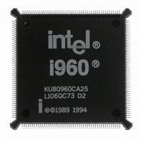
KU80960CA25 Intel, KU80960CA25 Datasheet - Page 28

KU80960CA25
Manufacturer Part Number
KU80960CA25
Description
IC MPU I960CA 5V 25MHZ 196QFP
Manufacturer
Intel
Datasheet
1.KU80960CA25.pdf
(68 pages)
Specifications of KU80960CA25
Rohs Status
RoHS non-compliant
Processor Type
i960
Features
CA suffix, 32-Bit with DMA
Speed
25MHz
Voltage
5V
Mounting Type
Surface Mount
Package / Case
196-QFP
Family Name
i960
Device Core Size
32b
Frequency (max)
25MHz
Instruction Set Architecture
RISC
Supply Voltage 1 (typ)
5V
Operating Supply Voltage (max)
5.5V
Operating Supply Voltage (min)
4.5V
Operating Temp Range
0C to 100C
Operating Temperature Classification
Commercial
Mounting
Surface Mount
Pin Count
196
Package Type
PQFP
Lead Free Status / Rohs Status
Not Compliant
Other names
802900
Available stocks
Company
Part Number
Manufacturer
Quantity
Price
Company:
Part Number:
KU80960CA25
Manufacturer:
INTEL
Quantity:
152
80960CA-33, -25, -16
(80960CA-33 only, under the conditions described in Section 4.2, Operating Conditions and Section 4.5.1, AC Test
Conditions.)
24
Relative Output Timings (1,2,3,8)
T
T
T
T
T
T
T
T
T
T
Relative Input Timings (1,2,3)
T
T
T
T
T
T
T
T
NOTES:
1. See Section 4.5.2, AC Timing Waveforms for waveforms and definitions.
2. See Figure 16 for capacitive derating information for output delays and hold times.
3. See Figure 17 for capacitive derating information for rise and fall times.
4. Where N is the number of N
5. N = Number of wait states inserted with READY.
6. Output Data and/or DT/R may be driven indefinitely following a cycle if there is no subsequent bus activity.
7. Since asynchronous inputs are synchronized internally by the 80960CA, they have no required setup or hold times to be recognized and for
8. These specifications are guaranteed by the processor.
9. These specifications must be met by the system for proper operation of the processor.
10. This timing is dependent upon the loading of PCLK2:1. Use the derating curves of Section 4.5.3, Derating Curves to adjust the timing for
11. In the 1-x input clock mode, the maximum input clock period is limited to 125 ns while the processor is operating. When the processor is in
12. When in the 1-x input clock mode, these specifications assume a stable input clock with a period variation of less than ± 0.1% between adja-
13. In 2-x clock mode, RESET is an asynchronous input which has no required setup and hold time for proper operation. However, to guarantee
14. In 1-x clock mode, RESET is an asynchronous input which has no required setup and hold time for proper operation. However, to guarantee
15. The interrupt pins are synchronized internally by the 80960CA. They have no required setup or hold times for proper operation. These pins
Symbol
AVSH1
AVSH2
AVEL1
AVEL2
NLQV
DVNH
NLNH
NHQX
EHTV
TVEL
IS5
IH5
IS6
IH6
IS7
IH7
IS8
IH8
active when there are no wait states in an access.
proper operation. However, to guarantee recognition of the input at a particular edge of PCLK2:1, the setup times shown must be met. Asyn-
chronous inputs must be active for at least two consecutive PCLK2:1 rising edges to be seen by the processor.
PCLK2:1 loading.
reset, the input clock may stop even in 1-x mode.
cent cycles.
the device exits reset synchronized to a particular clock edge, the RESET pin must meet setup and hold times to the falling edge of the
CLKIN. (See Figure 22.)
the device exits reset synchronized to a particular clock edge, the RESET pin must meet setup and hold times to the rising edge of the CLKIN.
(See Figure 23.)
are sampled by the interrupt controller every other clock and must be active for at least three consecutive PCLK2:1 rising edges when assert-
ing them asynchronously. To guarantee recognition at a particular clock edge, the setup and hold times shown must be met for two consecu-
tive PCLK2:1 rising edges.
A31:2 Valid to ADS Rising
BE3:0, W/R, SUP, D/C,
DMA, DACK3:0 Valid to ADS Rising
A31:2 Valid to DEN Falling
BE3:0, W/R, SUP, INST,
DMA, DACK3:0 Valid to DEN Falling
WAIT Falling to Output Data Valid
Output Data Valid to WAIT Rising
WAIT Falling to WAIT Rising
Output Data Hold after WAIT Rising
DT/R Hold after DEN High
DT/R Valid to DEN Falling
RESET Input Setup (2-x Clock Mode)
RESET Input Hold (2-x Clock Mode)
DREQ3:0 Input Setup
DREQ3:0 Input Hold
XINT7:0, NMI Input Setup
XINT7:0, NMI Input Hold
RESET Input Setup (1-x Clock Mode)
RESET Input Hold (1-x Clock Mode)
Table 16. 80960CA AC Characteristics (33 MHz) (Continued)
RAD
, N
RDD
, N
Parameter
WAD
or N
WDD
wait states that are programmed in the Bus Controller Region Table. WAIT never goes
(N+1)*T–8
N*T – 4
T/2 – 7
T/2 – 4
T/4 + 1
T – 4
T – 6
T – 4
T – 6
Min
12
6
5
7
7
3
3
N*T ± 4
± 4
(N+1)*T+6
N*T + 4
T + 4
T + 6
T + 4
T + 6
Max
ns
ns
ns
ns
ns
ns
ns
ns
ns
ns
ns
ns
ns
ns
ns
ns
ns
ns
Units
(4)
(4)
(5)
(6)
(13)
(13)
(7)
(7)
(15)
(15)
(14)
(14)
Notes


