MPC8260AVVPJDB Freescale Semiconductor, MPC8260AVVPJDB Datasheet - Page 3
MPC8260AVVPJDB
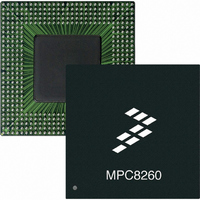
Manufacturer Part Number
MPC8260AVVPJDB
Description
IC MPU POWERQUICC II 480-TBGA
Manufacturer
Freescale Semiconductor
Datasheet
1.MPC8255ACVVMHBB.pdf
(50 pages)
Specifications of MPC8260AVVPJDB
Processor Type
MPC82xx PowerQUICC II 32-bit
Speed
300MHz
Voltage
2V
Mounting Type
Surface Mount
Package / Case
480-TBGA
Family Name
MPC82XX
Device Core
PowerQUICC II
Device Core Size
32b
Frequency (max)
300MHz
Instruction Set Architecture
RISC
Operating Supply Voltage (max)
2.2V
Operating Supply Voltage (min)
1.9V
Operating Temp Range
0C to 105C
Operating Temperature Classification
Commercial
Mounting
Surface Mount
Pin Count
480
Package Type
TBGA
For Use With
MPC8260ADS-TCOM - BOARD DEV ADS POWERQUICC II
Lead Free Status / RoHS Status
Lead free / RoHS Compliant
Features
-
Lead Free Status / Rohs Status
Compliant
Available stocks
Company
Part Number
Manufacturer
Quantity
Price
Company:

Part Number:
MPC8260AVVPJDB
Manufacturer:
Rohm
Quantity:
2 595
Company:
Part Number:
MPC8260AVVPJDB
Manufacturer:
FREESCALE
Quantity:
173
Company:
Part Number:
MPC8260AVVPJDB
Manufacturer:
Freescale Semiconductor
Quantity:
10 000


Freescale Semiconductor
•
•
•
•
•
•
•
MPC8260A PowerQUICC™ II Integrated Communications Processor Hardware Specifications, Rev. 2.0
— PowerPC architecture-compliant memory management unit (MMU)
— Common on-chip processor (COP) test interface
— High-performance (6.6–7.65 SPEC95 benchmark at 300 MHz; 1.68 MIPs/MHz without
— Supports bus snooping for data cache coherency
— Floating-point unit (FPU)
Separate power supply for internal logic and for I/O
Separate PLLs for G2 core and for the CPM
— G2 core and CPM can run at different frequencies for power/performance optimization
— Internal core/bus clock multiplier that provides 1.5:1, 2:1, 2.5:1, 3:1, 3.5:1, 4:1, 5:1, 6:1 ratios
— Internal CPM/bus clock multiplier that provides 2:1, 2.5:1, 3:1, 3.5:1, 4:1, 5:1, 6:1 ratios
64-bit data and 32-bit address 60x bus
— Bus supports multiple master designs
— Supports single- and four-beat burst transfers
— 64-, 32-, 16-, and 8-bit port sizes controlled by on-chip memory controller
— Supports data parity or ECC and address parity
32-bit data and 18-bit address local bus
— Single-master bus, supports external slaves
— Eight-beat burst transfers
— 32-, 16-, and 8-bit port sizes controlled by on-chip memory controller
60x-to-PCI bridge (MPC8265 and MPC8266 only)
— Programmable host bridge and agent
— 32-bit data bus, 66 MHz, 3.3 V
— Synchronous and asynchronous 60x and PCI clock modes
— All internal address space available to external PCI host
— DMA for memory block transfers
— PCI-to-60x address remapping
System interface unit (SIU)
— Clock synthesizer
— Reset controller
— Real-time clock (RTC) register
— Periodic interrupt timer
— Hardware bus monitor and software watchdog timer
— IEEE Std. 1149.1™ standard JTAG test access port
Twelve-bank memory controller
— Glueless interface to SRAM, page mode SDRAM, DRAM, EPROM, Flash and other user-
— Byte write enables and selectable parity generation
inlining and 1.90 Dhrystones MIPS/MHz with
definable peripherals
Features
3
Related parts for MPC8260AVVPJDB
Image
Part Number
Description
Manufacturer
Datasheet
Request
R

Part Number:
Description:
Manufacturer:
Freescale Semiconductor, Inc
Datasheet:
Part Number:
Description:
Manufacturer:
Freescale Semiconductor, Inc
Datasheet:
Part Number:
Description:
Manufacturer:
Freescale Semiconductor, Inc
Datasheet:
Part Number:
Description:
Manufacturer:
Freescale Semiconductor, Inc
Datasheet:
Part Number:
Description:
Manufacturer:
Freescale Semiconductor, Inc
Datasheet:
Part Number:
Description:
Manufacturer:
Freescale Semiconductor, Inc
Datasheet:
Part Number:
Description:
Manufacturer:
Freescale Semiconductor, Inc
Datasheet:
Part Number:
Description:
Manufacturer:
Freescale Semiconductor, Inc
Datasheet:
Part Number:
Description:
Manufacturer:
Freescale Semiconductor, Inc
Datasheet:
Part Number:
Description:
Manufacturer:
Freescale Semiconductor, Inc
Datasheet:
Part Number:
Description:
Manufacturer:
Freescale Semiconductor, Inc
Datasheet:
Part Number:
Description:
Manufacturer:
Freescale Semiconductor, Inc
Datasheet:
Part Number:
Description:
Manufacturer:
Freescale Semiconductor, Inc
Datasheet:
Part Number:
Description:
Manufacturer:
Freescale Semiconductor, Inc
Datasheet:
Part Number:
Description:
Manufacturer:
Freescale Semiconductor, Inc
Datasheet: