MPC8540PX667LB Freescale Semiconductor, MPC8540PX667LB Datasheet - Page 3
MPC8540PX667LB
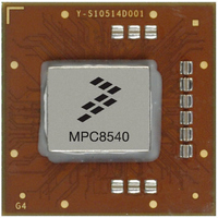
Manufacturer Part Number
MPC8540PX667LB
Description
IC MPU 32BIT 667MHZ 783-FCPBGA
Manufacturer
Freescale Semiconductor
Specifications of MPC8540PX667LB
Processor Type
MPC85xx PowerQUICC III 32-Bit
Speed
667MHz
Voltage
1.2V
Mounting Type
Surface Mount
Package / Case
783-FCPBGA
For Use With
MPC8548CDS - DEV TOOLS CDS FOR 8548MPC8540ADS-BGA - BOARD APPLICATION DEV 8540CWH-PPC-8540N-VE - KIT EVAL SYSTEM MPC8540
Lead Free Status / RoHS Status
Contains lead / RoHS non-compliant
Features
-
Available stocks
Company
Part Number
Manufacturer
Quantity
Price
Company:

Part Number:
MPC8540PX667LB
Manufacturer:
Freescale Semiconductor
Quantity:
10 000


Freescale Semiconductor
•
•
•
Section 3.1, “e500 Core Overview,” in the reference manual includes a comprehensive list of e500 core
features.
256-Kbyte L2 cache/SRAM
— Can be configured as follows:
— Full error checking and correction (ECC) support on 64-bit boundary in both cache and SRAM modes
— Cache mode supports instruction caching, data caching, or both
— External masters can force data to be allocated into the cache through programmed memory ranges or
— Eight-way set-associative cache organization (1024 sets of 32-byte cache lines)
— Supports locking the entire cache or selected lines. Individual line locks are set and cleared through
— Global locking and flash clearing done through writes to L2 configuration registers
— Instruction and data locks can be flash cleared separately
— Read and write buffering for internal bus accesses
— SRAM features include the following:
Address translation and mapping unit (ATMU)
— Eight local access windows define mapping within local 32-bit address space
— Inbound and outbound ATMUs map to larger external address spaces
DDR memory controller
— Programmable timing supporting DDR-1 SDRAM
— 64-bit data interface, up to 333-MHz data rate
— Four banks of memory supported, each up to 1 Gbyte
— DRAM chip configurations from 64 Mbits to 1 Gbit with x8/x16 data ports
— Full ECC support
— Page mode support (up to 16 simultaneous open pages)
— Contiguous or discontiguous memory mapping
— Read-modify-write support for RapidIO atomic increment, decrement, set, and clear transactions
— Sleep mode support for self-refresh SDRAM
– Full cache mode (256-Kbyte cache)
– Full memory-mapped SRAM mode (256-Kbyte SRAM mapped as a single 256-Kbyte block or two
– Half SRAM and half cache mode (128-Kbyte cache and 128-Kbyte memory-mapped SRAM)
special transaction types (stashing).
Book E instructions or by externally mastered transactions.
– I/O devices access SRAM regions by marking transactions as snoopable (global).
– Regions can reside at any aligned location in the memory map.
– Byte-accessible ECC is protected using read-modify-write transactions accesses for smaller than
– Three inbound windows plus a configuration window on PCI/PCI-X
– Four inbound windows plus a default and configuration window on RapidIO
– Four outbound windows plus default translation for PCI
– Eight outbound windows plus default translation for RapidIO
128-Kbyte blocks)
cache-line accesses
MPC8540 PowerQUICC III™ Integrated Host Processor Product Brief, Rev. 0.1
MPC8540 Overview
3
Related parts for MPC8540PX667LB
Image
Part Number
Description
Manufacturer
Datasheet
Request
R

Part Number:
Description:
Manufacturer:
Freescale Semiconductor, Inc
Datasheet:
Part Number:
Description:
Manufacturer:
Freescale Semiconductor, Inc
Datasheet:
Part Number:
Description:
Manufacturer:
Freescale Semiconductor, Inc
Datasheet:
Part Number:
Description:
Manufacturer:
Freescale Semiconductor, Inc
Datasheet:
Part Number:
Description:
Manufacturer:
Freescale Semiconductor, Inc
Datasheet:
Part Number:
Description:
Manufacturer:
Freescale Semiconductor, Inc
Datasheet:
Part Number:
Description:
Manufacturer:
Freescale Semiconductor, Inc
Datasheet:
Part Number:
Description:
Manufacturer:
Freescale Semiconductor, Inc
Datasheet:
Part Number:
Description:
Manufacturer:
Freescale Semiconductor, Inc
Datasheet:
Part Number:
Description:
Manufacturer:
Freescale Semiconductor, Inc
Datasheet:
Part Number:
Description:
Manufacturer:
Freescale Semiconductor, Inc
Datasheet:
Part Number:
Description:
Manufacturer:
Freescale Semiconductor, Inc
Datasheet:
Part Number:
Description:
Manufacturer:
Freescale Semiconductor, Inc
Datasheet:
Part Number:
Description:
Manufacturer:
Freescale Semiconductor, Inc
Datasheet:
Part Number:
Description:
Manufacturer:
Freescale Semiconductor, Inc
Datasheet: