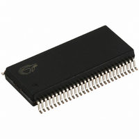
CY7C66113C-PVXC Cypress Semiconductor Corp, CY7C66113C-PVXC Datasheet - Page 16

CY7C66113C-PVXC
Manufacturer Part Number
CY7C66113C-PVXC
Description
IC MCU 8K USB HUB 4 PORT 56TSSOP
Manufacturer
Cypress Semiconductor Corp
Specifications of CY7C66113C-PVXC
Applications
USB Hub/Microcontroller
Core Processor
M8
Program Memory Type
OTP (8 kB)
Controller Series
USB Hub
Ram Size
256 x 8
Interface
I²C, USB, HAPI
Number Of I /o
31
Voltage - Supply
4 V ~ 5.5 V
Operating Temperature
0°C ~ 70°C
Mounting Type
Surface Mount
Package / Case
56-SSOP
No. Of I/o's
31
Eeprom Memory Size
8KB
Ram Memory Size
256Byte
Cpu Speed
48MHz
Digital Ic Case Style
SSOP
Supply
RoHS Compliant
Core Size
8bit
Program Memory Size
8KB
Oscillator Type
External, Internal
Peripherals
DAC
Rohs Compliant
Yes
Controller Family/series
(8051) USB
Embedded Interface Type
HAPI, I2C, USB
Processor Series
CY7C66xx
Core
M8
Data Bus Width
16 bit
Data Ram Size
256 B
Interface Type
HAPI, I2C, USB
Maximum Clock Frequency
12 MHz
Number Of Programmable I/os
39
Number Of Timers
1
Maximum Operating Temperature
+ 70 C
Mounting Style
SMD/SMT
Development Tools By Supplier
CY3654, CY3654-P03
Minimum Operating Temperature
0 C
Lead Free Status / RoHS Status
Lead free / RoHS Compliant
For Use With
CY3649 - PROGRAMMER HI-LO USB M8428-1339 - KIT LOW SPEED PERSONALITY BOARD
Lead Free Status / Rohs Status
Details
Other names
428-1808
Available stocks
Company
Part Number
Manufacturer
Quantity
Price
Company:
Part Number:
CY7C66113C-PVXC
Manufacturer:
HITTITE
Quantity:
101
Part Number:
CY7C66113C-PVXC
Manufacturer:
CIRRUS
Quantity:
20 000
Port 1Data
Port 2 Data
Port 3 Data
Special care should be taken with any unused GPIO data bits.
An unused GPIO data bit, either a pin on the chip or a port bit
that is not bonded on a particular package, must not be left
floating when the device enters the suspend state. If a GPIO data
bit is left floating, the leakage current caused by the floating bit
may violate the suspend current limitation specified by the USB
specifications. If a ‘1’ is written to the unused data bit and the port
is configured with open drain outputs, the unused data bit
remains in an indeterminate state. Therefore, if an unused port
bit is programmed in open-drain mode, it must be written with a
‘0.’ Notice that the CY7C66013C always requires that P3[7:5] be
written with a ‘0.’ When the CY7C66113C is used the P3[7]
should be written with a ‘0.’
Document Number: 38-08024 Rev. *D
Port 0 Data
Bit #
Bit Name
Read/Write
Reset
Bit #
Bit Name
Read/Write
Reset
Bit #
Bit Name
Read/Write
Reset
Bit #
Bit Name
Read/Write
Reset
7
P0.7
R/W
1
7
P1.7
R/W
1
7
P2.7
R/W
1
7
Reserved
R/W
-
6
P1.6
1
6
P0.6
R/W
1
R/W
6
P2.6
R/W
1
6
P3.6
CY7C66113C
only
R/W
1
P0.5
R/W
5
P1.5
R/W
1
5
P2.5
R/W
1
5
1
5
P3.5
CY7C66113C
only
R/W
1
Figure 10. Port 2 Data
Figure 11. Port 3 Data
Figure 8. Port 0 Data
Figure 9. Port1 Data
4
P1.4
R/W
1
4
P0.4
R/W
1
4
P2.4
R/W
1
4
P3.4
R/W
1
In normal non HAPI mode, reads from a GPIO port always return
the present state of the voltage at the pin, independent of the
settings in the Port Data Registers. If HAPI mode is activated for
a port, reads of that port return latched data as controlled by the
HAPI signals (see
During reset, all of the GPIO pins are set to a high impedance
input state (‘1’ in open drain mode). Writing a ‘0’ to a GPIO pin
drives the pin LOW. In this state, a ‘0’ is always read on that GPIO
pin unless an external source overdrives the internal pull down
device.
3
P1.3
R/W
1
3
P2.3
R/W
1
3
P0.3
R/W
1
3
P3.3
R/W
1
CY7C66013C, CY7C66113C
Hardware Assisted Parallel Interface
2
P1.2
R/W
1
2
P0.2
R/W
1
2
P2.2
R/W
1
2
P3.2
R/W
1
1
P1.1
R/W
1
1
P2.1
R/W
1
1
P0.1
R/W
1
1
P3.1
R/W
1
ADDRESS 0x03
ADDRESS 0x00
ADDRESS 0x01
ADDRESS 0x02
0
P1.0
R/W
1
0
P2.0
R/W
1
0
P0.0
R/W
1
Page 16 of 59
0
P3.0
R/W
1
(HAPI)).
[+] Feedback


