CY7C66113C-PVXC Cypress Semiconductor Corp, CY7C66113C-PVXC Datasheet - Page 14
CY7C66113C-PVXC
Manufacturer Part Number
CY7C66113C-PVXC
Description
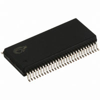
IC MCU 8K USB HUB 4 PORT 56TSSOP
Manufacturer
Cypress Semiconductor Corp
Specifications of CY7C66113C-PVXC
Applications
USB Hub/Microcontroller
Core Processor
M8
Program Memory Type
OTP (8 kB)
Controller Series
USB Hub
Ram Size
256 x 8
Interface
I²C, USB, HAPI
Number Of I /o
31
Voltage - Supply
4 V ~ 5.5 V
Operating Temperature
0°C ~ 70°C
Mounting Type
Surface Mount
Package / Case
56-SSOP
No. Of I/o's
31
Eeprom Memory Size
8KB
Ram Memory Size
256Byte
Cpu Speed
48MHz
Digital Ic Case Style
SSOP
Supply
RoHS Compliant
Core Size
8bit
Program Memory Size
8KB
Oscillator Type
External, Internal
Peripherals
DAC
Rohs Compliant
Yes
Controller Family/series
(8051) USB
Embedded Interface Type
HAPI, I2C, USB
Processor Series
CY7C66xx
Core
M8
Data Bus Width
16 bit
Data Ram Size
256 B
Interface Type
HAPI, I2C, USB
Maximum Clock Frequency
12 MHz
Number Of Programmable I/os
39
Number Of Timers
1
Maximum Operating Temperature
+ 70 C
Mounting Style
SMD/SMT
Development Tools By Supplier
CY3654, CY3654-P03
Minimum Operating Temperature
0 C
Lead Free Status / RoHS Status
Lead free / RoHS Compliant
For Use With
CY3649 - PROGRAMMER HI-LO USB M8428-1339 - KIT LOW SPEED PERSONALITY BOARD
Lead Free Status / Rohs Status
Details
Other names
428-1808
Available stocks
Company
Part Number
Manufacturer
Quantity
Price
Company:

Part Number:
CY7C66113C-PVXC
Manufacturer:
HITTITE
Quantity:
101
Part Number:
CY7C66113C-PVXC
Manufacturer:
CIRRUS
Quantity:
20 000


Reset
The CY7C66x13C supports two resets: POR and a Watchdog
Reset (WDR). Each of these resets causes:
■
■
■
■
The occurrence of a reset is recorded in the Processor Status
and Control Register, as described in
Control Register
occurrence of POR and WDR, respectively. Firmware
interrogates these bits to determine the cause of a reset.
Program execution starts at ROM address 0x0000 after a reset.
Although this looks similar to interrupt vector 0, there is an
important difference. Reset processing does NOT push the
program counter, carry flag, and zero flag onto program stack.
The firmware reset handler should configure the hardware
before the “main” loop of code. Attempting to execute a RET or
RETI in the firmware reset handler causes unpredictable
execution results.
Power on Reset
When V
and the CY7C66x13C enters a “semi-suspend” state. During the
semi-suspend state, which is different from the suspend state
defined in the USB specification, the oscillator and all other
blocks of the part are functional, except for the CPU. This
semi-suspend time ensures that both a valid V
and that the internal PLL has time to stabilize before full
operation begins. When the V
2.5V, and the oscillator is stable, the POR is deasserted and the
on-chip timer starts counting. The first 1 ms of suspend time is
Document Number: 38-08024 Rev. *D
All registers to be restored to their default states.
The USB device addresses to be set to 0.
All interrupts to be disabled.
The PSP and DSP to be set to memory address 0x00.
CC
is first applied to the chip, the POR signal is asserted
on page 26. Bits 4 and 6 are used to record the
Last write to
WDT
Register
CC
rises above approximately
Processor Status and
CC
level is reached
t
WATCH
Figure 6. Watchdog Reset
No write to WDT
register, so WDR
goes HIGH
not interruptible, and the semi-suspend state continues for an
additional 95 ms unless the count is bypassed by a USB Bus
Reset on the upstream port. The 95 ms provides time for V
stabilize at a valid operating voltage before the chip executes
code.
If a USB Bus Reset occurs on the upstream port during the 95
ms semi-suspend time, the semi-suspend state is aborted and
program execution begins immediately from address 0x0000. In
this case, the Bus Reset interrupt is pending but not serviced
until firmware sets the USB Bus Reset Interrupt Enable bit (bit 0
of register 0x20) and enables interrupts with the EI command.
The POR signal is asserted whenever V
approximately 2.5V, and remains asserted until V
this level again. Behavior is the same as described earlier.
Watchdog Reset
The WDR occurs when the internal WDT rolls over. Writing any
value to the write only Watchdog Restart Register at address
0x26 clears the timer. The timer rolls over and WDR occurs if it
is not cleared within t
6 of the Processor Status and Control Register is set to record
this event (the register contents are set to 010X0001 by the
WDR). A WDT Reset lasts for 2 ms, after which the
microcontroller begins execution at ROM address 0x0000.
The USB transmitter is disabled by a WDR because the USB
Device Address Registers are cleared (see
Addresses). Otherwise, the USB Controller responds to all
address 0 transactions.
It is possible to set the WDR bit of the Processor Status and
Control Register (0xFF) following a POR event. If a firmware
interrogates the Processor Status and Control Register for a set
condition on the WDR bit, the WDR bit should be ignored if the
POR (bit 3 of register 0xFF) bit is set.
2 ms
Execution begins at
Reset Vector 0x0000
CY7C66013C, CY7C66113C
WATCH
(8 ms minimum) of the last clear. Bit
CC
CC
Page 14 of 59
USB Device
drops below
rises above
CC
to
[+] Feedback
Related parts for CY7C66113C-PVXC
Image
Part Number
Description
Manufacturer
Datasheet
Request
R

Part Number:
Description:
IC MCU 8K USB HUB 4 PORT 56TSSOP
Manufacturer:
Cypress Semiconductor Corp
Datasheet:

Part Number:
Description:
Manufacturer:
Cypress Semiconductor Corp
Datasheet:
Part Number:
Description:
Manufacturer:
Cypress Semiconductor Corp
Datasheet:
Part Number:
Description:
Manufacturer:
Cypress Semiconductor Corp
Datasheet:
Part Number:
Description:
Manufacturer:
Cypress Semiconductor Corp
Datasheet:
Part Number:
Description:
Manufacturer:
Cypress Semiconductor Corp
Datasheet: