CY7C66113C-PVXC Cypress Semiconductor Corp, CY7C66113C-PVXC Datasheet
CY7C66113C-PVXC
Specifications of CY7C66113C-PVXC
Available stocks


Related parts for CY7C66113C-PVXC


CY7C66113C-PVXC Summary of contents
Page 1
... Full-Speed USB (12 Mbps) Peripheral Controller with Integrated Hub Cypress Semiconductor Corporation Document #: 38-08024 Rev. *B Full-Speed USB (12 Mbps) Peripheral Controller with Integrated Hub • 198 Champion Court • San Jose CY7C66013C CY7C66113C , CA 95134-1709 • 408-943-2600 Revised January 2, 2006 ...
Page 2
... DAC Isink Registers ...............................................................................................................26 10.2 DAC Port Interrupts ................................................................................................................26 11.0 12-BIT FREE-RUNNING TIMER ................................................................................................. AND HAPI CONFIGURATION REGISTER ...........................................................................27 2 13.0 I C-COMPATIBLE CONTROLLER .............................................................................................28 14.0 HARDWARE ASSISTED PARALLEL INTERFACE (HAPI) .......................................................30 15.0 PROCESSOR STATUS AND CONTROL REGISTER ................................................................31 Document #: 38-08024 Rev. *B TABLE OF CONTENTS CY7C66013C CY7C66113C Page ...
Page 3
... USB MODE TABLES ..................................................................................................................47 21.0 REGISTER SUMMARY ...............................................................................................................51 22.0 SAMPLE SCHEMATIC ................................................................................................................53 23.0 ABSOLUTE MAXIMUM RATINGS ..............................................................................................54 24.0 ELECTRICAL CHARACTERISTICS ...........................................................................................54 25.0 SWITCHING CHARACTERISTICS .............................................................................................55 26.0 ORDERING INFORMATION .......................................................................................................57 27.0 PACKAGE DIAGRAMS ...............................................................................................................58 28.0 QUAD FLAT PACKAGE NO LEADS (QFN) PACKAGE DESIGN NOTES ................................59 Document #: 38-08024 Rev. *B CY7C66013C CY7C66113C Page ...
Page 4
... Figure 3-1. CY7C66113C 56-pin QFN Pin Assignment .......................................................................11 Figure 3-2. CY7C66113C DIE ..............................................................................................................12 Figure 5-1. Program Memory Space with Interrupt Vector Table .........................................................18 Figure 6-1. Clock Oscillator On-Chip Circuit ........................................................................................20 Figure 7-1. Watchdog Reset ................................................................................................................21 Figure 9-1. Block Diagram of a GPIO Pin ............................................................................................22 Figure 9-2. Port 0 Data ........................................................................................................................23 Figure 9-3 ...
Page 5
... Table 19-1. Memory Allocation for Endpoints ......................................................................................42 Table 20-1. USB Register Mode Encoding ..........................................................................................47 Table 20-2. Decode Table for Table 20-3: “Details of Modes for Differing Traffic Conditions” ............48 Table 20-3. Details of Modes for Differing Traffic Conditions ...............................................................49 Document #: 38-08024 Rev. *B LIST OF TABLES CY7C66013C CY7C66113C Page ...
Page 6
... Higher current drive achievable by connecting multiple GPIO pins together to drive a common output — Each GPIO port can be configured as inputs with internal pull-ups or open drain outputs or traditional CMOS outputs — A Digital-to-Analog Conversion (DAC) port with programmable current sink outputs is available on the CY7C66113C device — ...
Page 7
... DAC The CY7C66113C has an additional port P4[7:0] that features an additional eight programmable sink current I/O pins (DAC). Every DAC pin includes an integrated 14-k disabled and the output pin is driven HIGH by the internal pull-up resistor. When a ‘0’ is written to a DAC I/O pin, the internal pull-up is disabled and the output pin provides the programmed amount of sink current. A DAC I/O pin can be used as an input with an internal pull-up by writing a ‘ ...
Page 8
... USB The CY7C66013C and CY7C66113C include an integrated USB Serial Interface Engine (SIE) that supports the integrated peripherals and the hub controller function. The hardware supports up to two USB device addresses with one device address for the hub (two endpoints) and a device address for a compound device (three endpoints). The SIE allows the USB host to commu- nicate with the hub and functions integrated into the microcontroller ...
Page 9
... P2[6]; CS P3[0] GPIO High Current Outputs PORT 3 P3[4] GPIO Additional P3[5] High Current PORT 3 P3[6] Outputs DAC[0] DAC PORT DAC[7] CY7C66113C only SCLK SDATA Interface 2 *I C-compatible interface enabled by firmware through P2[1:0] or P1[1:0] CY7C66013C CY7C66113C D+[0] Upstream USB Port D–[0] USB D+[1] D– ...
Page 10
... P3[4] P3[ D–[4] D+[ D+[4] D–[ P2[0] P2[ P2[2] D+[ GND D–[ P2[4] P2[ P2[6] P2[ P2[ P0[0] DAC[ P0[2] P0[ P0[4] P0[ P0[6] P0[3] P0[1] DAC[5] DAC[3] DAC[1] CY7C66013C CY7C66113C CY7C66113C 56-pin SSOP P1[ P1[0] 4 P1[2] 53 P1[ P1[ P3[ D–[ D+[ P3[ P3[ D–[ D+[ P3[ P2[ P2[ GND 18 39 P2[4] ...
Page 11
... D+[1] 5 D–[1] 6 P2[1] 7 D+[2] 8 D–[2] 9 P2[3] 10 P2[5] 11 P2[7] 12 DAC[7] 13 P0[7] 14 Figure 3-1. CY7C66113C 56-pin QFN Pin Assignment Document #: 38-08024 Rev. *B CY7C66113C 56-pin QFN CY7C66013C CY7C66113C P3[0] 42 D–[3] 41 D+[3] 40 P3[2] 39 P3[4] 38 D–[4] 37 D+[4] 36 P3[6] ...
Page 12
... Cypress Logo Pin 15 Pin 30 (0,0) Document #: 38-08024 Rev. *B Pin 1 Pin 60 Pin 45 DIE STEP: 3398 x 4194 microns Die Size: 3322 x 4129 microns Die Thickness: 14 mils = 355.6 microns Pad Size microns Figure 3-2. CY7C66113C DIE CY7C66013C CY7C66113C (3398, 4194) Page ...
Page 13
... CY7C66013C CY7C66113C Pin Name X Y DAC6 2000.6 210.6 DAC4 2103.6 210.6 DAC2 2206.6 210.6 Port06 2308.4 210.6 Port04 2411.4 210.6 Port02 2514.4 210.6 Port00 2617.4 210.6 Vpp 2992 ...
Page 14
... GPIO Port 1 Data 0x02 R/W GPIO Port 2 Data 0x03 R/W GPIO Port 3 Data 0x04 W Interrupt Enable for Pins in Port 0 0x05 W Interrupt Enable for Pins in Port 1 0x06 W Interrupt Enable for Pins in Port 2 0x07 W Interrupt Enable for Pins in Port 3 CY7C66013C CY7C66113C Description Function Page Page ...
Page 15
... Hub Downstream Port Suspend Control 0x4E R Hub Downstream Ports Resume Status 0x4F R Hub Downstream Ports SE0 Status 0x50 R Hub Downstream Ports Differential data 0x51 R/W Hub Downstream Ports Force LOW 0xFF R/W Microprocessor Status and Control Register CY7C66013C CY7C66113C Function 2 C Position Configuration Page Page ...
Page 16
... AND [expr],A 5 AND [X+expr],A 7 XOR [expr],A 8 XOR [X+expr],A 4 IOWX [X+expr] 5 CPL 6 ASL 4 ASR 5 RLC RRC 4 RET RETI JNC 10 JACC 5 INDEX 5 CY7C66013C CY7C66113C operand opcode cycles 20 4 acc direct 23 7 index 24 8 acc direct 27 7 index 28 8 address 29 5 address 2A 5 ...
Page 17
... CALL instruction. The program counter, carry flag, and zero flag are restored from the program stack during a RETI instruction. Only the program counter is restored during a RET instruction. The program counter cannot be accessed directly by the firmware. The program stack can be examined by reading SRAM from location 0x00 and up. Document #: 38-08024 Rev. *B CY7C66013C CY7C66113C Page ...
Page 18
... USB address B endpoint 0 interrupt vector 0x0010 USB address B endpoint 1 interrupt vector 0x0012 Hub interrupt vector 0x0014 DAC interrupt vector 0x0016 GPIO/HAPI interrupt vector 2 0x0018 I C interrupt vector 0x001A Program Memory begins here 0x1FDF 8 KB (-32) PROM ends here. CY7C66013C CY7C66113C Page ...
Page 19
... Endpoint sizes are fixed by the Endpoint Size Bit (I/O register 0x1F, Bit 7), see Table 19-1 . Document #: 38-08024 Rev. *B Address Program Stack Growth 0x00 user selected User variables USB FIFO space for up to two Addresses and five endpoints 0xFF CY7C66013C CY7C66113C Data Stack Growth Page [2] ...
Page 20
... MOV A,20h; Move 20 hex into Accumulator (must be D8h or less) SWAP A,DSP; swap accumulator value into DSP register. 5.6 Address Modes The CY7C66013C and CY7C66113C microcontrollers support three addressing modes for instructions that require data operands: data, direct, and indexed. 5.6.1 Data (Immediate) “ ...
Page 21
... WATCH No write to WDT register, so WDR goes HIGH Figure 7-1. Watchdog Reset CY7C66013C CY7C66113C level is reached and CC has risen above approximately 2.5V, and CC rises above this level minimum) of the last clear. Bit WATCH Execution begins at ...
Page 22
... Interrupt Enable Interrupt Controller Document #: 38-08024 Rev mode 2-bits Q2 Q1 Data Out Latch 14 k Q3* Data In Latch Data Interrupt Latch Figure 9-1. Block Diagram of a GPIO Pin CY7C66013C CY7C66113C or Gnd. This also CC GPIO PIN *Port 0,1,2: Low I sink Port 3: High I sink Page ...
Page 23
... If a ‘1’ is written to the unused data bit and the port is configured with open drain outputs, the unused data bit remains in an indeterminate state. Therefore unused port bit is programmed in open-drain mode, it must be written with a ‘0.’ Notice that the CY7C66013C always requires that P3[7:5] be written with a ‘0.’ When the CY7C66113C is used the P3[7] should be written with a ‘0.’ ...
Page 24
... Hi-Z 0 Output LOW 1 Hi P0.5 Intr P0.4 Intr P0.3 Intr Enable Enable Enable Figure 9-7. Port 0 Interrupt Enable CY7C66013C CY7C66113C Interrupt Polarity 0 Disabled 1 – (Falling Edge) 0 Disabled 1 Disabled 0 Disabled 1 – (Falling Edge) 0 Disabled 1 + (Rising Edge) ADDRESS 0x04 P0.2 Intr P0.1 Intr P0 ...
Page 25
... DAC Port The CY7C66113CC features a programmable sink current 8 bit port which is also known as DAC port. Each of these port I/O pins have a programmable current sink. Writing a ‘1’ DAC I/O pin disables the output current sink (I pin HIGH through an integrated 14-k resistor is disabled ...
Page 26
... Enable Bit 5 Enable Bit 4 Enable Bit Figure 10-4. DAC Port Interrupt Enable Polarity Bit 5 Polarity Bit 4 Polarity Bit Figure 10-5. DAC Port Interrupt Polarity CY7C66013C CY7C66113C ADDRESS 0x30 DAC[2] DAC[1] DAC[0] R/W R/W R ADDRESS 0x38 –0x3F Isink[2] Isink[1] Isink[ ADDRESS 0x31 ...
Page 27
... Figure 11-3. Timer Block Diagram [3] . All bits of this register are cleared on reset LEMPTY DRDY Latch Polarity Polarity Empty R/W R Figure 12-1. HAPI/I C Configuration Register CY7C66013C CY7C66113C ADDRESS 0x24 Timer Bit 2 Timer Bit 1 Timer Bit ADDRESS 0x25 Timer Bit 10 Timer Bit 9 Timer Bit 8 R ...
Page 28
... Figure 13- Data Register ACK Addr R/W R/W R Figure 13- Status and Control Register CY7C66013C CY7C66113C 2 C-compatible interfaces. HAPI Port Width Position P2[1:0], 0:SCL, 1:SDA P1[1:0], 0:SCL, 1:SDA P2[1:0], 0:SCL, 1:SDA 2 C Status and Control Register 2 C Status and Control 2 C SDA data is connected to bit 1 of GPIO port ...
Page 29
... C-compatible block to initiate a master mode transaction by sending a start bit and 2 C-compatible block performs any required arbitration and clock synchronization. IN the 2 C Stop bit is generated restart sequence. The I CY7C66013C CY7C66113C 2 C GPIO pins operate 2 C Status and Control register. This 2 C-compatible bus at the ACK bit 2 C start or restart ...
Page 30
... If 0, Data Ready is active LOW, DReadyPin is active HIGH Data Ready is active HIGH, DReadyPin is active LOW. Determines polarity of Latch Empty bit and LatEmptyPin Latch Empty is active LOW, LatEmptyPin is active HIGH Latch Empty is active HIGH, LatEmptyPin is active LOW. CY7C66013C CY7C66113C 2 C-compatible bus Page ...
Page 31
... Interrupt Enable Register. Writing a ‘1’ bit position enables the interrupt associated with that bit position. Document #: 38-08024 Rev USB Bus Reset Power-On Suspend Interrupt Reset R/W R/W R C-compatible or HAPI operation, the internal USB hub, or CY7C66013C CY7C66113C ADDRESS 0xFF Interrupt Reserved Run Enable Sense R R/W R minimum) WATCH Page ...
Page 32
... Enable Interrupt Enable R/W R/W R Figure 16-1. Global Interrupt Enable Register Reserved EPB1 Interrupt EPB0 Interrupt Enable Enable - R/W R CY7C66013C CY7C66113C ADDRESS 0X20 1.024-ms 128- s USB Bus RST Interrupt Interrupt Interrupt Enable Enable Enable R/W R/W R ADDRESS 0X21 EPA2 Interrupt EPA1 Interrupt ...
Page 33
... Bit AddrB EP1 CLR AddrB EP1 IRQ CLR Hub CLR Hub IRQ Interrupt DAC CLR DAC IRQ Acknowledge GPIO/HAPI CLR GPIO/HAPI IRQ CLR IRQ Interrupt Priority Encoder CY7C66013C CY7C66113C IRQ Sense IRQ Int Enable Sense Controlled by DI, EI, and RETI Instructions Page ...
Page 34
... USB Address A Endpoint 0 interrupt 0x000A USB Address A Endpoint 1 interrupt 0x000C USB Address A Endpoint 2 interrupt 0x000E USB Address B Endpoint 0 interrupt 0x0010 USB Address B Endpoint 1 interrupt 0x0012 USB Hub interrupt 0x0014 DAC interrupt 0x0016 GPIO/HAPI interrupt 2 0x0018 I C interrupt CY7C66013C CY7C66113C Function Page ...
Page 35
... Section 14.0. Document #: 38-08024 Rev. *B Port OR Gate (1 input per GPIO pin) 1 Global 1 = Enable GPIO Interrupt 0 = Disable Enable (Bit 5, Register 0x20) Figure 16-4. GPIO Interrupt Structure CY7C66013C CY7C66113C GPIO Interrupt Flip Flop Interrupt D Q Priority Encoder CLR Page IRQout Interrupt Vector ...
Page 36
... C-compatible bus to signal the need for firmware interaction. This generally 2 2 C-compatible bus and leave the I C-compatible hardware in the idle state. 2 C-compatible bus to generate the interrupt interrupt occurs. CY7C66013C CY7C66113C 2 C registers. Refer 2 C register contents may be must be placed in series ext Page ...
Page 37
... These features are mapped onto a hub repeater and a hub controller. The hub controller is supported by the processor integrated into the CY7C66013C and CY7C66113C microcontrollers. The hardware in the hub repeater detects whether a USB device is connected to a downstream port and the interface speed of the downstream device. The connection to a downstream port is through a differential signal pair (D+ and D– ...
Page 38
... Port 4 Speed R/W R/W R Figure 18-2. Hub Ports Speed Reserved Reserved Port 4 Enable R/W R/W R Figure 18-3. Hub Ports Enable Register CY7C66013C CY7C66113C ADDRESS 0x48 Port 3 Connect Port 2 Connect Port 1 Connect Status Status Status R/W R/W R ADDRESS 0x4A Port 3 Speed Port 2 Speed ...
Page 39
... R/W R/W R Figure 18-5. Hub Ports Force Low Register Reserved Reserved Port 4 SE0 Status - - Figure 18-6. Hub Ports SE0 Status Register CY7C66013C CY7C66113C ADDRESS 0x4B Port 2 Port 1 Port 1 Control Bit 0 Control Bit 1 Control Bit 0 R/W R/W R ADDRESS 0x51 Force Low Force Low Force Low D– ...
Page 40
... Reserved Reserved Port 4 Selective Suspend R/W R/W R Figure 18-8. Hub Ports Suspend Register Reserved Reserved Resume Figure 18-9. Hub Ports Resume Status Register CY7C66013C CY7C66113C ADDRESS 0x50 ADDRESS 0x4D Port 3 Port 2 Port 1 Selective Selective Selective Suspend Suspend Suspend R/W R/W R/W ...
Page 41
... Force D+[0] LOW, D–[0] HiZ 111 Force D+[0] HiZ, D–[0] HiZ Document #: 38-08024 Rev D– Upstream Bus Activity Figure 18-10. USB Status and Control Register Control Action CY7C66013C CY7C66113C ADDRESS 0x1F Control Action Control Action Control Action Bit 2 Bit 1 Bit 0 R/W R/W R Page ...
Page 42
... One USB Address Endpoints) Start Address Size Label 0xA8 8 EPA4 0xB0 8 EPA3 0xB8 8 EPA2 0xC0 32 EPA1 0xE0 32 EPA0 CY7C66013C CY7C66113C ADDRESSES 0x10(A) and 0x40( Device Device Address Address Bit 2 Bit 1 R/W R [0,1] [1,1] One USB Address Endpoints) Start Start Address Size ...
Page 43
... Control Write transfer a USB host were to immediately start the next transfer, the new Setup packet could override the data payload of the data stage of the previous Control Write. Document #: 38-08024 Rev Endpoint 0 OUT ACK Mode Bit 3 Received R/W R/W R Figure 19-2. USB Endpoint 0 Mode Registers CY7C66013C CY7C66113C ADDRESSES 0x12(A0) and 0x42(B0 Mode Bit 2 Mode Bit 1 Mode Bit 0 R/W R/W R Page ...
Page 44
... Byte Count Bit Byte Count Bit Byte Count Bit R/W R/W R Figure 19-4. USB Endpoint Counter Registers CY7C66013C CY7C66113C ADDRESSES 0x14, 0x16, 0x44 Mode Bit 2 Mode Bit 1 Mode Bit 0 R/W R/W R ADDRESSES 0x11, 0x13, 0x15, 0x41, 0x43 Byte Count Bit Byte Count Bit ...
Page 45
... For details on what conditions are required to generate an endpoint interrupt, refer to Table 20-2. 4. The contents of the updated endpoint 0 mode and counter registers are locked, except the SETUP bit of the endpoint 0 mode register which was locked earlier. Document #: 38-08024 Rev. *B CY7C66013C CY7C66113C Page ...
Page 46
... UPDATE Host To Device Data 1/0 Data Packet SETUP Host To Device Data 1/0 Data Packet Figure 19-5. Token/Data Packet Flow Diagram CY7C66013C CY7C66113C Host To Device Hand Shake Packet UPDATE Device To Host ACK NAK STAL 16 C Hand Shake UPDATE Packet UPDATE only if FIFO is ...
Page 47
... Is set by SIE on an ACK from mode 1101 (Ack In) TX count ignore On issuance of an ACK this mode is changed by SIE to 1100 (NAK In) stall ignore check Is set by SIE on an ACK from mode 1111 (Ack In – Status Out) – Status Out) CY7C66013C CY7C66113C Comments Page ...
Page 48
... Setup Byte Count (bits 0..5, Figure 17-4) Data Valid (bit 6, Figure 17-4) Data0/1 (bit7 Figure 17-4) PID Status Bits (Bit[7..5], Figure The validity of the received data 17-2) CY7C66013C CY7C66113C In Out ACK Response SIE’s Response to the Host Endpoint Mode bits Changed by the SIE ...
Page 49
... Changes made by SIE to Internal Registers and Mode Bits dval DTOG DVAL COUNT Setup In Out ACK Mode Bits Response Intr valid 1 1 updates UC valid 0 1 updates UC valid updates 1 updates invalid CY7C66013C CY7C66113C ACK Changeignore Changeignore Changeignore ChangeNAK ChangeNAK Changeignore Changeignore ChangeStall ChangeStall UC 1 ...
Page 50
... UC UC invalid ENDPOINT Changes made by SIE to Internal Registers and Mode Bits dval DTOG DVAL COUNT Setup In Out ACK Mode Bits Response Intr CY7C66013C CY7C66113C ACK (back) yes ChangeACK Stall Stall Changeignore Changeignore ChangeNAK ChangeACK Stall Stall Changeignore Changeignore Stall ACK Changeignore ...
Page 51
... Byte Count Count Count Bit 5 Bit 4 Bit ACK Mode Bit 3 Mode Bit 2 Mode Bit 1 Mode Bit 0 bbbbbbbb Endpoint D+ D– Bus Mode Upstream Upstream Activity CY7C66013C CY7C66113C ChangeNAK Changeignore ChangeTX Read/Write [ Bit 2 Bit 1 Bit 0 /Both P0.2 P0.1 P0.0 bbbbbbbb P1.2 P1.1 P1 ...
Page 52
... Diff. Data Force Low Force Low Force Low Force Low D–[4] D+[3] D–[3] D+[2] WDR USB Bus Power-on Suspend Interrupt Reset In- Reset terrupt CY7C66013C CY7C66113C Read/Write [ Bit 2 Bit 1 Bit 0 /Both 1.024-ms 128- s USB Bus -bbbbbbb Interrupt Interrupt RESET Enable Enable Interrupt ...
Page 53
... D0– D1– D0+ D1+ D2– XTALO D2+ D3– XTALI D3+ GND GND D4– Vpp D4+ 15K(x8 UDN POWER MANAGEMENT Figure 22-1. Sample Schematic CY7C66013C CY7C66113C ) Page USB-A Vbus D– D+ GND USB-A Vbus D– D+ GND USB-A Vbus D– D+ GND USB-A Vbus D– D+ GND ...
Page 54
... USB pins Linear ramp ±5% to Gnd 1.5 k ± REF Including R Resistor ext All ports, LOW to HIGH edge All ports, HIGH to LOW edge below approximately 2.5V. CC CY7C66013C CY7C66113C = 4.0V to 5.25V) CC Min. Max. 3.15 3.45 –0.4 0 0.2 0.8 2.5 0.8 2.0 20 –10 10 ...
Page 55
... DC out V = 2.0V DC out [11 2.0V DC out [12 2.0V out V = 2.0V DC out [13] DAC Port (F = 6.0 MHz) OSC Description / [15, 16] [16] [15, 16] [16] [16] [15, 16] CY7C66013C CY7C66113C = 4.0V to 5.25V) (continued) CC Min. Max. Unit 2.4 V 8.0 24.0 k 0.1 0.3 mA 0.5 1.5 mA 1.6 4 1.6 4.8 mA 0.6 LSB Min. ...
Page 56
... Internal Write Internal Addr Figure 25-3. HAPI Read by External Interface from USB Microcontroller Document #: 38-08024 Rev CYC Figure 25-1. Clock Timing t r 90% 90% 10% Figure 25-2. USB Data Signal Timing t t OED t OEDR (Ready) Port0 CY7C66013C CY7C66113C t r 10% Int RD D[23:0] t OEZ Page ...
Page 57
... LEMPTY Polarity=0) Internal Read Internal Addr Figure 25-4. HAPI Write by External Device to USB Microcontroller 26.0 Ordering Information Ordering Code PROM Size CY7C66013C-PVXC 8 KB CY7C66113C-PVXC 8 KB CY7C66113C-LFXC 8 KB CY7C66113C-PVXCT 8 KB CY7C66113C- Document #: 38-08024 Rev D[23:0] t DSTB t STBLE (not empty) Package Type ...
Page 58
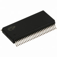
... Package Diagrams Document #: 38-08024 Rev. *B 48-pin Shrunk Small Outline Package O48 56-pin Shrunk Small Outline Package O56 CY7C66013C CY7C66113C 51-85061-*C 51-85062-*C Page ...
Page 59
... Document #: 38-08024 Rev. *B 56-Lead QFN LF56A SIDE VIEW 0.08[0.003] C 1.00[0.039] MAX. 0.05[0.002] MAX. 0.80[0.031] MAX. 0.20[0.008] REF. 0.30[0.012] 0.50[0.020] 0°-12° C SEATING PLANE CY7C66013C CY7C66113C BOTTOM VIEW 0.18[0.007] 0.28[0.011] PIN1 ID N 0.20[0.008 0.45[0.018] E-PAD (PAD SIZE VARY BY DEVICE TYPE) 0.24[0.009] (4X) 0.60[0.024] ...
Page 60
... Solder Mask Cu Fill Cu Fill 0.013” dia PCB Material This figure only shows the top three layers of the circuit board: Top Solder, PCB Dielectric, and the Ground Plane 2 C system, provided that the system conforms to the I CY7C66013C CY7C66113C 2 C Standard Specification Page ...
Page 61
... Document History Page Document Title: CY7C66013C, CY7C66113C Full-Speed USB (12 Mbps) Peripheral Controller with Integrated Hub Document Number: 38-08024 Issue REV. ECN NO. Date ** 114525 3/27/02 *A 124768 03/20/03 *B 417632 See ECN Document #: 38-08024 Rev. *B Orig. of Change Description of Change DSG Change from Spec number: 38-00591 to 38-08024 MON Added register bit definitions ...