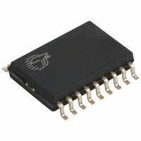
CY7C63723-SC Cypress Semiconductor Corp, CY7C63723-SC Datasheet - Page 5

CY7C63723-SC
Manufacturer Part Number
CY7C63723-SC
Description
IC MCU 8K LS USB/PS-2 18-SOIC
Manufacturer
Cypress Semiconductor Corp
Series
enCoRe™r
Specifications of CY7C63723-SC
Applications
USB Microcontroller
Core Processor
M8B
Program Memory Type
OTP (8 kB)
Controller Series
CY7C637xx
Ram Size
256 x 8
Interface
PS2, USB
Number Of I /o
10
Voltage - Supply
4 V ~ 5.5 V
Operating Temperature
0°C ~ 70°C
Mounting Type
Surface Mount
Package / Case
18-SOIC (7.5mm Width)
Lead Free Status / RoHS Status
Contains lead / RoHS non-compliant
Other names
428-1323
Available stocks
Company
Part Number
Manufacturer
Quantity
Price
Company:
Part Number:
CY7C63723-SC
Manufacturer:
CYPRESS
Quantity:
3 100
Company:
Part Number:
CY7C63723-SC
Manufacturer:
FUJI
Quantity:
154
Part Number:
CY7C63723-SC
Manufacturer:
CYPRESS/赛普拉斯
Quantity:
20 000
6.6.2
“Direct” address mode is used when the data operand is a
variable stored in SRAM. In that case, the one byte address of
the variable is encoded in the instruction. As an example,
consider an instruction that loads A with the contents of
memory address location 0x10h:
In normal usage, variable names are assigned to variable
addresses using “EQU” statements to improve the readability
of the assembler source code. As an example, the following
code is equivalent to the example shown above.
7.0
Refer to the CYASM Assembler User’s Guide for detailed
information on these instructions. Note that conditional jump
instructions (i.e., JC, JNC, JZ, JNZ) take five cycles if jump is
taken, four cycles if no jump.
Document #: 38-08022 Rev. *B
HALT
ADD A,expr
ADD A,[expr]
ADD A,[X+expr]
ADC A,expr
ADC A,[expr]
ADC A,[X+expr]
SUB A,expr
SUB A,[expr]
SUB A,[X+expr]
SBB A,expr
SBB A,[expr]
SBB A,[X+expr]
OR A,expr
OR A,[expr]
OR A,[X+expr]
AND A,expr
AND A,[expr]
AND A,[X+expr]
XOR A,expr
XOR A,[expr]
XOR A,[X+expr]
CMP A,expr
CMP A,[expr]
CMP A,[X+expr]
MOV A,expr
• DSPINIT: EQU 30h
• MOV A,DSPINIT
• MOV A, [10h]
• buttons: EQU 10h
• MOV A, [buttons]
MNEMONIC
Direct
Instruction Set Summary
data
direct
index
data
direct
index
data
direct
index
data
direct
index
data
direct
index
data
direct
index
data
direct
index
data
direct
index
data
Operand
00
01
02
03
04
05
06
07
08
09
0A
0B
0C
0D
0E
0F
10
11
12
13
14
15
16
17
18
19
FOR
FOR
Opcode
7
4
6
7
4
6
7
4
6
7
4
6
7
4
6
7
4
6
7
4
6
7
5
7
8
4
Cycles
NOP
INC A
INC X
INC [expr]
INC [X+expr]
DEC A
DEC X
DEC [expr]
DEC [X+expr]
IORD expr
IOWR expr
POP A
POP X
PUSH A
PUSH X
SWAP A,X
SWAP A,DSP
MOV [expr],A
MOV [X+expr],A
OR [expr],A
OR [X+expr],A
AND [expr],A
AND [X+expr],A
XOR [expr],A
XOR [X+expr],A
IOWX [X+expr]
6.6.3
“Indexed” address mode allows the firmware to manipulate
arrays of data stored in SRAM. The address of the data
operand is the sum of a constant encoded in the instruction
and the contents of the “X” register. In normal usage, the
constant will be the “base” address of an array of data and the
X register will contain an index that indicates which element of
the array is actually addressed.
This would have the effect of loading A with the fourth element
of the SRAM “array” that begins at address 0x10h. The fourth
element would be at address 0x13h.
• array: EQU 10h
• MOV X,3
• MOV A, [x+array]
MNEMONIC
Indexed
acc
x
direct
index
acc
x
direct
index
address
address
direct
index
direct
index
direct
index
direct
index
index
Operand
20
21
22
23
24
25
26
27
28
29
2A
2B
2C
2D
2E
2F
30
31
32
33
34
35
36
37
38
39
Opcode
CY7C63722
CY7C63723
CY7C63743
Page 5 of 49
4
4
4
7
8
4
4
7
8
5
5
4
4
5
5
5
5
5
6
7
8
7
8
7
8
6
Cycles


