CY7C63723-SC Cypress Semiconductor Corp, CY7C63723-SC Datasheet - Page 39
CY7C63723-SC
Manufacturer Part Number
CY7C63723-SC
Description
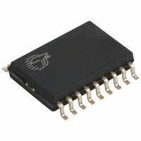
IC MCU 8K LS USB/PS-2 18-SOIC
Manufacturer
Cypress Semiconductor Corp
Series
enCoRe™r
Specifications of CY7C63723-SC
Applications
USB Microcontroller
Core Processor
M8B
Program Memory Type
OTP (8 kB)
Controller Series
CY7C637xx
Ram Size
256 x 8
Interface
PS2, USB
Number Of I /o
10
Voltage - Supply
4 V ~ 5.5 V
Operating Temperature
0°C ~ 70°C
Mounting Type
Surface Mount
Package / Case
18-SOIC (7.5mm Width)
Lead Free Status / RoHS Status
Contains lead / RoHS non-compliant
Other names
428-1323
Available stocks
Company
Part Number
Manufacturer
Quantity
Price
Company:

Part Number:
CY7C63723-SC
Manufacturer:
CYPRESS
Quantity:
3 100
Company:
Part Number:
CY7C63723-SC
Manufacturer:
FUJI
Quantity:
154
Part Number:
CY7C63723-SC
Manufacturer:
CYPRESS/赛普拉斯
Quantity:
20 000


25.0
Note:
Document #: 38-08022 Rev. *B
11. The 200 Ω internal resistance at the VREG pin gives a standard USB pull-up using this value. Alternately, a 1.5 k Ω ,5%pull-up from D– to an external 3.3V supply
V
V
V
V
V
C
I
R
R
V
R
R
V
V
V
V
V
V
V
V
V
R
LO
OLU
OHZ
DI
CM
SE
OLP
ICR
ICF
HC
ITTL
OL1A
OL1B
OL2
OL3
OH
IN
PU
PD
PS2
UP
XIN
can be used.
DC Characteristics
Static Output Low
Static Output High, idle or suspend
Differential Input Sensitivity
Differential Input Common Mode Range
Single Ended Receiver Threshold
Transceiver Capacitance
Hi-Z State Data Line Leakage
External Bus Pull-up resistance (D–)
External Bus Pull-down resistance
Static Output Low
Internal PS/2 Pull-up Resistance
Pull-up Resistance
Input Threshold Voltage, CMOS mode
Input Threshold Voltage, CMOS mode
Input Hysteresis Voltage, CMOS mode
Input Threshold Voltage, TTL mode
Output Low Voltage, high drive mode
Output Low Voltage, medium drive mode
Output Low Voltage, low drive mode
Output High Voltage, strong drive mode
Pull-down resistance, XTALIN pin
General Purpose I/O Interface
PS/2 Interface
Parameter
FOSC = 6 MHz; Operating Temperature = 0 to 70°C (continued)
FOR
FOR
With R
R
connected D– to VREG pin
|(D+)–(D–)|
0 V < V
1.3 kΩ ±2% to V
15 kΩ ±5% to Gnd
Isink = 5 mA, SDATA or SCLK pins
SDATA, SCLK pins, PS/2 Enabled
Low to high edge, Port 0 or 1
High to low edge, Port 0 or 1
High to low edge, Port 0 or 1
Ports 0, 1, and 2
I
I
I
I
Port 0 or 1, I
Internal Clock Mode only
OL1
OL1
OL2
OL3
PD
connected D– to Gnd, R
= 50 mA, Ports 0 or 1
= 25 mA, Ports 0 or 1
= 8 mA, Ports 0 or 1
= 2 mA, Ports 0 or 1
PU
in
<3.3 V (D+ or D– pins)
to VREG pin
OH
Conditions
= 2 mA
REG
[11]
[4]
[4]
[4]
[4]
[4]
[4]
PU
V
1.274
14.25
40%
35%
Min.
–10
CC
3%
2.7
0.2
0.8
0.8
0.8
50
3
8
–2
CY7C63722
CY7C63723
CY7C63743
1.326
15.75
Max.
60%
55%
10%
0.4
0.3
3.6
2.5
2.0
2.0
0.8
0.4
0.4
0.4
20
10
24
7
Page 39 of 49
Unit
V
V
V
µA
kΩ
kΩ
pF
kΩ
kΩ
kΩ
V
V
V
V
V
V
V
V
V
V
V
V
CC
CC
CC
Related parts for CY7C63723-SC
Image
Part Number
Description
Manufacturer
Datasheet
Request
R

Part Number:
Description:
Manufacturer:
Cypress Semiconductor Corp
Datasheet:
Part Number:
Description:
Manufacturer:
Cypress Semiconductor Corp
Datasheet:
Part Number:
Description:
Manufacturer:
Cypress Semiconductor Corp
Datasheet:
Part Number:
Description:
Manufacturer:
Cypress Semiconductor Corp
Datasheet:
Part Number:
Description:
Manufacturer:
Cypress Semiconductor Corp
Datasheet: