20-101-1112 Rabbit Semiconductor, 20-101-1112 Datasheet - Page 99
20-101-1112
Manufacturer Part Number
20-101-1112
Description
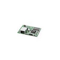
MODULE RABBITCORE RCM4010
Manufacturer
Rabbit Semiconductor
Datasheet
1.20-101-1094.pdf
(130 pages)
Specifications of 20-101-1112
Module/board Type
MPU Core Module
Product
Microcontroller Modules
Core Processor
Rabbit 4000
Clock Speed
58.98 MHz
Interface Type
Ethernet, Serial
Flash
512 KB
Timers
10 x 8 bit, 1 x 10 bit, 1 x 16 bit
Operating Supply Voltage
3 V to 3.6 V
Board Size
47 mm x 61 mm x 20 mm
Core
RCM4010
Processor Series
RCM4000
Silicon Manufacturer
Rabbit
Core Architecture
Rabbit 4000
Silicon Core Number
RCM4010
Silicon Family Name
RCM4000
Kit Contents
Board
Development Tool Type
Hardware / Software - Dev Kit (Dev Tool)
Rohs Compliant
Yes
For Use With/related Products
RCM4010
Lead Free Status / RoHS Status
Lead free / RoHS Compliant
Other names
Q3413688


Table A-8 lists the delays in gross memory access time for several values of VDD
The measurements are taken at the 50% points under the following conditions.
• T = -40°C to 85°C, V = VDD
• Internal clock to nonloaded CLK pin delay 1 ns @ 85°C/3.0 V
The clock to address output delays are similar, and apply to the following delays.
• T
• T
• T
• T
• T
• T
The data setup time delays are similar for both T
When the spectrum spreader is enabled with the clock doubler, every other clock cycle is
shortened (sometimes lengthened) by a maximum amount given in the table above. The
shortening takes place by shortening the high part of the clock. If the doubler is not
enabled, then every clock is shortened during the low part of the clock period. The maxi-
mum shortening for a pair of clocks combined is shown in the table.
Rabbit’s Technical Note TN227, Interfacing External I/O with Rabbit Microprocessor
Designs, contains suggestions for interfacing I/O devices to the Rabbit 4000 microproces-
sors.
User’s Manual
VDD
(V)
adr
3.3
1.8
CSx
IOCSx
IORD
IOWR
BUFEN
, the clock to address delay
IO
, the clock to memory chip select delay
, the clock to I/O read strobe delay
, the clock to I/O write strobe delay
, the clock to I/O chip select delay
, the clock to I/O buffer enable delay
30 pF 60 pF 90 pF
Clock to Address
18
6
Output Delay
Table A-8. Preliminary Data and Clock Delays
(ns)
24
8
11
33
IO
Data Setup
Time Delay
±10%
(ns)
1
3
0.5 ns setting
setup
no dbl / dbl
2.3 / 2.3
7 / 6.5
and T
Spectrum Spreader Delay
hold
.
Worst-Case
1 ns setting
no dbl / dbl
3 / 4.5
8 / 12
(ns)
2 ns setting
no dbl / dbl
11 / 22
4.5 / 9
IO
.
93
Related parts for 20-101-1112
Image
Part Number
Description
Manufacturer
Datasheet
Request
R

Part Number:
Description:
COMPUTER SGL-BRD BL2500 29.4MHZ
Manufacturer:
Rabbit Semiconductor
Datasheet:

Part Number:
Description:
COMPUTER SGL-BRD BL2500 29.4MHZ
Manufacturer:
Rabbit Semiconductor
Datasheet:

Part Number:
Description:
DISPLAY GRAPHIC 12KEY PROG OP670
Manufacturer:
Rabbit Semiconductor
Datasheet:
Part Number:
Description:
DISPLAY GRAPHIC 12KEY ETH OP6700
Manufacturer:
Rabbit Semiconductor
Datasheet:

Part Number:
Description:
COMPUTER SINGLE-BOARD BL2030
Manufacturer:
Rabbit Semiconductor
Part Number:
Description:
COMPUTER SGL-BOARD ETH BL2010
Manufacturer:
Rabbit Semiconductor

Part Number:
Description:
MODULE OP6810 W/O ETH/MEM EXPANS
Manufacturer:
Rabbit Semiconductor
Datasheet:
Part Number:
Description:
COMPUTER SINGLE-BOARD BL2020
Manufacturer:
Rabbit Semiconductor
Part Number:
Description:
COMPUTER BL2010 W/FRICTION LOCK
Manufacturer:
Rabbit Semiconductor
Part Number:
Description:
COMPUTER BL2020 W/FRICTION LOCK
Manufacturer:
Rabbit Semiconductor
Part Number:
Description:
COMPUTER SGL-BRD BL2500 44.2MHZ
Manufacturer:
Rabbit Semiconductor
Datasheet:
Part Number:
Description:
COMPUTER SGL-BOARD FULL BL2000
Manufacturer:
Rabbit Semiconductor

Part Number:
Description:
COMPUTER SINGLE-BOARD BL2110
Manufacturer:
Rabbit Semiconductor

Part Number:
Description:
COMPUTER SGL-BRD 29.4MHZ BL2610
Manufacturer:
Rabbit Semiconductor
Datasheet:
Part Number:
Description:
INTERFACE OP6800 512K FLASH&SRAM
Manufacturer:
Rabbit Semiconductor
Datasheet: