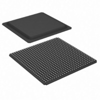
XC2VP30-6FGG676C Xilinx Inc, XC2VP30-6FGG676C Datasheet - Page 129

XC2VP30-6FGG676C
Manufacturer Part Number
XC2VP30-6FGG676C
Description
IC FPGA VIRTEX-II PRO 676-FBGA
Manufacturer
Xilinx Inc
Series
Virtex™-II Pror
Datasheet
1.XC2VP20-5FGG676C.pdf
(430 pages)
Specifications of XC2VP30-6FGG676C
Number Of Logic Elements/cells
30816
Number Of Labs/clbs
3424
Total Ram Bits
2506752
Number Of I /o
416
Voltage - Supply
1.425 V ~ 1.575 V
Mounting Type
Surface Mount
Operating Temperature
0°C ~ 85°C
Package / Case
676-BBGA
Lead Free Status / RoHS Status
Lead free / RoHS Compliant
Number Of Gates
-
Available stocks
Company
Part Number
Manufacturer
Quantity
Price
Company:
Part Number:
XC2VP30-6FGG676C
Manufacturer:
XILINX
Quantity:
490
Part Number:
XC2VP30-6FGG676C
Manufacturer:
XILINX/赛灵思
Quantity:
20 000
- Current page: 129 of 430
- Download datasheet (4Mb)
DS083 (v4.7) November 5, 2007
This document provides Virtex™-II Pro Device/Package
Combinations, Maximum I/Os, and Virtex-II Pro Pin Defini-
tions, followed by pinout tables, for these packages:
•
•
•
•
•
Virtex-II Pro Device/Package Combinations and Maximum I/Os
Wire-bond and flip-chip packages are available.
Table 2
wire-bond and flip-chip packages, respectively.
•
•
•
Table 2: Flip-Chip Packages Information
Table 3
and the number of differential I/O pairs for each Virtex-II Pro device/package combination. The number of I/Os per package
includes all user I/Os except the fifteen control pins (CCLK, DONE, M0, M1, M2, PROG_B, PWRDWN_B, TCK, TDI, TDO,
TMS, HSWAP_EN, DXN, DXP, and RSVD), the nine (per transceiver) RocketIO MGT pins (TXP, TXN, RXP, RXN,
AVCCAUXTX, AVCCAUXRX, VTTX, VTRX, and GNDA), and for Virtex-II Pro X devices only, the two BREFCLKN/
BREFCLKP differential clock input pairs (four pins). The Virtex-II Pro X devices are highlighted in bold type.
1. Unless otherwise noted, "Virtex-II Pro" refers to members of the Virtex-II Pro and/or Virtex-II Pro X families.
© 2002–2007 Xilinx, Inc. All rights reserved. XILINX, the Xilinx logo, the Brand Window, and other designated brands included herein are trademarks of Xilinx, Inc. PowerPC is
a trademark of IBM Corp. and is used under license. All other trademarks are the property of their respective owners.
DS083 (v4.7) November 5, 2007
Product Specification
Pitch (mm)
Size (mm)
Maximum I/Os
FG256/FGG256 Fine-Pitch BGA Package
FG456/FGG456 Fine-Pitch BGA Package
FG676/FGG676 Fine-Pitch BGA Package
FF672 Flip-Chip Fine-Pitch BGA Package
FF896 Flip-Chip Fine-Pitch BGA Package
FG denotes wire-bond fine-pitch BGA
(1.00 mm pitch).
FGG denotes Pb-free wire-bond fine-pitch BGA
(1.00 mm pitch).
FF denotes flip-chip fine-pitch BGA
(1.00 mm pitch)
Package
shows the number of available I/Os, the number of RocketIO™ (or RocketIO X) multi-gigabit transceiver (MGT) pins,
show the maximum number of user I/Os possible in
27 x 27
FF672
1.00
396
R
3
0
2
31 x 31
FF896
Virtex-II Pro and Virtex-II Pro X Platform FPGAs:
1.00
556
Table 1
FF1152
35 x 35
1.00
www.xilinx.com
644
and
•
•
•
•
•
For device pinout diagrams and layout guidelines, refer to
the
pinout files are also available for download from the Xilinx
website (
.
Table 1: Wire-Bond Packages Information
Notes:
1. Wire-bond packages include FGGnnn Pb-free versions. See
Pitch (mm)
Size (mm)
Maximum I/Os
FF1148
35 x 35
Virtex-II Pro Platform FPGA User Guide
FF1152 Flip-Chip Fine-Pitch BGA Package
FF1148 Flip-Chip Fine-Pitch BGA Package
FF1517 Flip-Chip Fine-Pitch BGA Package
FF1704 Flip-Chip Fine-Pitch BGA Package
FF1696 Flip-Chip Fine-Pitch BGA Package
Virtex-II Pro Ordering Examples (Module
Package
1.00
812
www.xilinx.com
(1)
FF1517
40 x 40
1.00
964
FGG256
FG256/
17 x 17
1.00
140
).
Pinout Information
(1)
42.5 x 42.5
FF1704
FGG456
1040
1.00
FG456/
23 x 23
Product Specification
1.00
248
1).
. ASCII package
42.5 x 42.5
Module 4 of 4
FF1696
FGG676
FG676/
26 x 26
1200
1.00
1.00
412
1
Related parts for XC2VP30-6FGG676C
Image
Part Number
Description
Manufacturer
Datasheet
Request
R

Part Number:
Description:
IC VIRTEXIIPRO FPGA 30K 676FCBGA
Manufacturer:
Xilinx Inc
Datasheet:

Part Number:
Description:
IC FPGA VIRTEX-II PRO 896-FBGA
Manufacturer:
Xilinx Inc
Datasheet:

Part Number:
Description:
IC FPGA VIRTEX-II PRO 1152-FBGA
Manufacturer:
Xilinx Inc
Datasheet:

Part Number:
Description:
IC FPGA VIRTEX-II PRO 676-FBGA
Manufacturer:
Xilinx Inc
Datasheet:

Part Number:
Description:
IC VIRTEXIIPRO FPGA 30K 896FCBGA
Manufacturer:
Xilinx Inc
Datasheet:

Part Number:
Description:
IC FPGA VIRTEX-II PRO 896-FBGA
Manufacturer:
Xilinx Inc
Datasheet:

Part Number:
Description:
IC FPGA VIRTEX-II PRO 1152-FBGA
Manufacturer:
Xilinx Inc
Datasheet:

Part Number:
Description:
IC FPGA VIRTEX-II PRO 676-FBGA
Manufacturer:
Xilinx Inc
Datasheet:

Part Number:
Description:
IC FPGA VIRTEX-II PRO 676-FBGA
Manufacturer:
Xilinx Inc
Datasheet:

Part Number:
Description:
IC FPGA VIRTEX-II PRO 896-FBGA
Manufacturer:
Xilinx Inc
Datasheet:

Part Number:
Description:
IC FPGA VIRTEX-II PRO 896-FBGA
Manufacturer:
Xilinx Inc
Datasheet:

Part Number:
Description:
IC FPGA VIRTEX-II PRO 1152-FBGA
Manufacturer:
Xilinx Inc
Datasheet:

Part Number:
Description:
IC FPGA VIRTEX-II PRO 1152-FBGA
Manufacturer:
Xilinx Inc
Datasheet:

Part Number:
Description:
IC FPGA VIRTEX-II PRO 676FGBGA
Manufacturer:
Xilinx Inc
Datasheet:

Part Number:
Description:
IC FPGA VIRTEX-II PRO 896FFBGA
Manufacturer:
Xilinx Inc
Datasheet:


