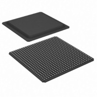
XC2VP30-6FGG676C Xilinx Inc, XC2VP30-6FGG676C Datasheet - Page 113

XC2VP30-6FGG676C
Manufacturer Part Number
XC2VP30-6FGG676C
Description
IC FPGA VIRTEX-II PRO 676-FBGA
Manufacturer
Xilinx Inc
Series
Virtex™-II Pror
Datasheet
1.XC2VP20-5FGG676C.pdf
(430 pages)
Specifications of XC2VP30-6FGG676C
Number Of Logic Elements/cells
30816
Number Of Labs/clbs
3424
Total Ram Bits
2506752
Number Of I /o
416
Voltage - Supply
1.425 V ~ 1.575 V
Mounting Type
Surface Mount
Operating Temperature
0°C ~ 85°C
Package / Case
676-BBGA
Lead Free Status / RoHS Status
Lead free / RoHS Compliant
Number Of Gates
-
Available stocks
Company
Part Number
Manufacturer
Quantity
Price
Company:
Part Number:
XC2VP30-6FGG676C
Manufacturer:
XILINX
Quantity:
490
Part Number:
XC2VP30-6FGG676C
Manufacturer:
XILINX/赛灵思
Quantity:
20 000
- Current page: 113 of 430
- Download datasheet (4Mb)
Global Clock Input to Output Delay for LVCMOS25, 12 mA, Fast Slew Rate,
Without DCM
Table 51: Global Clock Input to Output Delay for LVCMOS25, 12 mA, Fast Slew Rate,
Without DCM
DS083 (v4.7) November 5, 2007
Product Specification
Notes:
1. Listed above are representative values where one global clock input drives one vertical clock line in each accessible column, and
2. Output timing is measured at 50% V
3. DCM output jitter is already included in the timing calculation.
LVCMOS25 Global Clock Input to Output
Delay using Output Flip-flop, 12 mA, Fast
Slew Rate, without DCM.
For data output with different standards,
adjust the delays with the values shown in
IOB Output Switching Characteristics
Standard Adjustments, page
Global Clock and OFF without DCM
where all accessible IOB and CLB flip-flops are clocked by the global clock net.
R
Description
26.
Virtex-II Pro and Virtex-II Pro X Platform FPGAs: DC and Switching Characteristics
CC
threshold with test setup shown in
Symbol
T
ICKOF
www.xilinx.com
XC2VPX20
XC2VPX70
XC2VP100
XC2VP20
XC2VP30
XC2VP40
XC2VP50
XC2VP70
XC2VP2
XC2VP4
XC2VP7
Device
Figure
6. For other I/O standards, see
3.19
3.39
3.59
3.62
3.62
3.73
3.89
4.00
4.38
4.38
N/A
-7
Speed Grade
3.52
3.91
4.00
4.08
4.08
4.12
4.28
4.43
4.87
4.87
5.32
-6
3.82
4.27
4.36
4.46
4.46
4.50
4.67
4.84
5.33
5.33
5.82
-5
Table
Module 3 of 4
37.
Units
ns
ns
ns
ns
ns
ns
ns
ns
ns
ns
ns
42
Related parts for XC2VP30-6FGG676C
Image
Part Number
Description
Manufacturer
Datasheet
Request
R

Part Number:
Description:
IC VIRTEXIIPRO FPGA 30K 676FCBGA
Manufacturer:
Xilinx Inc
Datasheet:

Part Number:
Description:
IC FPGA VIRTEX-II PRO 896-FBGA
Manufacturer:
Xilinx Inc
Datasheet:

Part Number:
Description:
IC FPGA VIRTEX-II PRO 1152-FBGA
Manufacturer:
Xilinx Inc
Datasheet:

Part Number:
Description:
IC FPGA VIRTEX-II PRO 676-FBGA
Manufacturer:
Xilinx Inc
Datasheet:

Part Number:
Description:
IC VIRTEXIIPRO FPGA 30K 896FCBGA
Manufacturer:
Xilinx Inc
Datasheet:

Part Number:
Description:
IC FPGA VIRTEX-II PRO 896-FBGA
Manufacturer:
Xilinx Inc
Datasheet:

Part Number:
Description:
IC FPGA VIRTEX-II PRO 1152-FBGA
Manufacturer:
Xilinx Inc
Datasheet:

Part Number:
Description:
IC FPGA VIRTEX-II PRO 676-FBGA
Manufacturer:
Xilinx Inc
Datasheet:

Part Number:
Description:
IC FPGA VIRTEX-II PRO 676-FBGA
Manufacturer:
Xilinx Inc
Datasheet:

Part Number:
Description:
IC FPGA VIRTEX-II PRO 896-FBGA
Manufacturer:
Xilinx Inc
Datasheet:

Part Number:
Description:
IC FPGA VIRTEX-II PRO 896-FBGA
Manufacturer:
Xilinx Inc
Datasheet:

Part Number:
Description:
IC FPGA VIRTEX-II PRO 1152-FBGA
Manufacturer:
Xilinx Inc
Datasheet:

Part Number:
Description:
IC FPGA VIRTEX-II PRO 1152-FBGA
Manufacturer:
Xilinx Inc
Datasheet:

Part Number:
Description:
IC FPGA VIRTEX-II PRO 676FGBGA
Manufacturer:
Xilinx Inc
Datasheet:

Part Number:
Description:
IC FPGA VIRTEX-II PRO 896FFBGA
Manufacturer:
Xilinx Inc
Datasheet:


