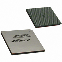
EP2S180F1508C4 Altera, EP2S180F1508C4 Datasheet - Page 138

EP2S180F1508C4
Manufacturer Part Number
EP2S180F1508C4
Description
IC STRATIX II FPGA 180K 1508FBGA
Manufacturer
Altera
Series
Stratix® IIr
Datasheet
1.EP2S15F484I4N.pdf
(238 pages)
Specifications of EP2S180F1508C4
Number Of Logic Elements/cells
179400
Number Of Labs/clbs
8970
Total Ram Bits
9383040
Number Of I /o
1170
Voltage - Supply
1.15 V ~ 1.25 V
Mounting Type
Surface Mount
Operating Temperature
0°C ~ 85°C
Package / Case
1508-FBGA
For Use With
544-1701 - DSP PRO KIT W/SII EP2S180N
Lead Free Status / RoHS Status
Contains lead / RoHS non-compliant
Number Of Gates
-
Other names
544-1416
Available stocks
Company
Part Number
Manufacturer
Quantity
Price
Part Number:
EP2S180F1508C4
Manufacturer:
ALTERA/阿尔特拉
Quantity:
20 000
Part Number:
EP2S180F1508C4ES
Manufacturer:
ALTERA/阿尔特拉
Quantity:
20 000
Company:
Part Number:
EP2S180F1508C4N
Manufacturer:
ALTERA
Quantity:
3 000
Part Number:
EP2S180F1508C4N
Manufacturer:
ALTERA/阿尔特拉
Quantity:
20 000
Operating Conditions
5–2
Stratix II Device Handbook, Volume 1
V
V
V
V
V
V
V
Symbol
Table 5–3. Stratix II Device Recommended Operating Conditions (Part 1 of 2)
CCINT
CCIO
CCPD
CCA
CCD
I
O
Supply voltage for internal logic
Supply voltage for input and
output buffers, 3.3-V operation
Supply voltage for input and
output buffers, 2.5-V operation
Supply voltage for input and
output buffers, 1.8-V operation
Supply voltage for output buffers,
1.5-V operation
Supply voltage for input and
output buffers, 1.2-V operation
Supply voltage for pre-drivers as
well as configuration and JTAG
I/O buffers.
Analog power supply for PLLs
Digital power supply for PLLs
Input voltage (see
Output voltage
Parameter
Table
Recommended Operating Conditions
Table 5–3
conditions.
Table 5–2. Maximum Duty Cycles in Voltage Transitions
Symbol
5–2)
V
I
contains the Stratix II device family recommended operating
Maximum duty cycles
in voltage transitions
100 μs ≤ risetime ≤ 100 ms
100 μs ≤ risetime ≤ 100 ms (3),
100 μs ≤ risetime ≤ 100 ms
100 μs ≤ risetime ≤ 100 ms
100 μs ≤ risetime ≤ 100 ms
100 μs ≤ risetime ≤ 100 ms
100 μs ≤ risetime ≤ 100 ms
100 μs ≤ risetime ≤ 100 ms
100 μs ≤ risetime ≤ 100 ms
(2),
(5)
Parameter
Conditions
Condition
V
V
V
V
V
V
I
I
I
I
I
I
(3)
(3)
(3)
(3)
(3)
(3)
(3)
(4)
= 4.0 V
= 4.1 V
= 4.2 V
= 4.3 V
= 4.4 V
= 4.5 V
(6)
Minimum
(3.00)
3.135
2.375
1.425
3.135
1.15
1.71
1.14
1.15
1.15
–0.5
0
Note (1)
Duty Cycles
Maximum
100
Altera Corporation
90
50
30
17
10
Maximum Unit
(3.60)
3.465
2.625
1.575
3.465
V
1.25
1.89
1.26
1.25
1.25
4.0
CCIO
April 2011
Unit
%
%
%
%
%
%
V
V
V
V
V
V
V
V
V
V
V


