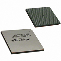
EP2S180F1508C4 Altera, EP2S180F1508C4 Datasheet - Page 102

EP2S180F1508C4
Manufacturer Part Number
EP2S180F1508C4
Description
IC STRATIX II FPGA 180K 1508FBGA
Manufacturer
Altera
Series
Stratix® IIr
Datasheet
1.EP2S15F484I4N.pdf
(238 pages)
Specifications of EP2S180F1508C4
Number Of Logic Elements/cells
179400
Number Of Labs/clbs
8970
Total Ram Bits
9383040
Number Of I /o
1170
Voltage - Supply
1.15 V ~ 1.25 V
Mounting Type
Surface Mount
Operating Temperature
0°C ~ 85°C
Package / Case
1508-FBGA
For Use With
544-1701 - DSP PRO KIT W/SII EP2S180N
Lead Free Status / RoHS Status
Contains lead / RoHS non-compliant
Number Of Gates
-
Other names
544-1416
Available stocks
Company
Part Number
Manufacturer
Quantity
Price
Part Number:
EP2S180F1508C4
Manufacturer:
ALTERA/阿尔特拉
Quantity:
20 000
Part Number:
EP2S180F1508C4ES
Manufacturer:
ALTERA/阿尔特拉
Quantity:
20 000
Company:
Part Number:
EP2S180F1508C4N
Manufacturer:
ALTERA
Quantity:
3 000
Part Number:
EP2S180F1508C4N
Manufacturer:
ALTERA/阿尔特拉
Quantity:
20 000
I/O Structure
2–94
Stratix II Device Handbook, Volume 1
Notes to
(1)
(2)
(3)
(4)
Table 2–18. Stratix II MultiVolt I/O Support
V
CCIO
1.2
1.5
1.8
2.5
3.3
To drive inputs higher than V
and LVCMOS input levels to overdrive input buffer option in the Quartus II software.
The pin current may be slightly higher than the default value. You must verify that the driving device’s V
maximum and V
voltage specifications.
Although V
a different level can still interface with the Stratix II device if it has inputs that tolerate the V
Stratix II devices do not support 1.2-V LVTTL and 1.2-V LVCMOS. Stratix II devices support 1.2-V HSTL.
(V)
Table
2–18:
1.2
(4)
(4)
(4)
(4)
CCIO
(4)
specifies the voltage necessary for the Stratix II device to drive out, a receiving device powered at
O H
v
minimum voltages do not violate the applicable Stratix II V
1.5
v
v
(2)
Input Signal (V)
Table 2–18
The TDO and nCEO pins are powered by V
in. TDO is in I/O bank 4 and nCEO is in I/O bank 7.
Ideally, the V
at the same voltage level. This may not always be possible depending on
the V
configuration voltage level chosen by VCCSEL on slave devices. Master
and slave devices can be in any position in the chain. Master indicates that
it is driving out TDO or nCEO to a slave device.
For multi-device passive configuration schemes, the nCEO pin of the
master device drives the nCE pin of the slave device. The VCCSEL pin on
the slave device selects which input buffer is used for nCE. When VCCSEL
is logic high, it selects the 1.8-V/1.5-V buffer powered by V
VCCSEL is logic low it selects the 3.3-V/2.5-V input buffer powered by
V
device match the VCCSEL settings for the nCE input buffer of the slave
device it is connected to, but that may not be possible depending on the
application.
ensure that nCEO can successfully drive nCE for all power supply
combinations.
CCPD
CCIO
v
1.8
v
v
CCIO
but less than 4.0 V, disable the PCI clamping diode and select the Allow LVTTL
. The ideal case is to have the V
(2)
level of TDO and nCEO pins on master devices and the
summarizes Stratix II MultiVolt I/O support.
Table 2–19
v
v
v
CC
2.5
v
v
(2)
(2)
(2)
supplies for the I/O buffers of any two connected pins are
Note (1)
v
v
v
3.3
v
v
contains board design recommendations to
(2)
(2)
(2)
v
v
v
v
v
1.2
(3)
(3)
(3)
(4)
(3)
CCIO
v
v
v
1.5
v
(3)
(3)
(3)
CCIO
of the nCEO bank in a master
Output Signal (V)
I L
of the bank that they reside
v
v
maximum and V
1.8
v
(3)
(3)
v
CCIO
Altera Corporation
2.5
v
(3)
value.
CCIO
I H
3.3
v
minimum
. When
May 2007
O L
5.0
v


