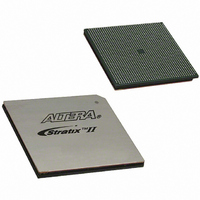
EP2S180F1508C4N Altera, EP2S180F1508C4N Datasheet - Page 176

EP2S180F1508C4N
Manufacturer Part Number
EP2S180F1508C4N
Description
IC STRATIX II FPGA 180K 1508FBGA
Manufacturer
Altera
Series
Stratix® IIr
Datasheet
1.EP2S15F484I4N.pdf
(238 pages)
Specifications of EP2S180F1508C4N
Number Of Logic Elements/cells
179400
Number Of Labs/clbs
8970
Total Ram Bits
9383040
Number Of I /o
1170
Voltage - Supply
1.15 V ~ 1.25 V
Mounting Type
Surface Mount
Operating Temperature
0°C ~ 85°C
Package / Case
1508-FBGA
Family Name
Stratix II
Number Of Logic Blocks/elements
179400
# I/os (max)
1170
Frequency (max)
711.24MHz
Process Technology
90nm (CMOS)
Operating Supply Voltage (typ)
1.2V
Logic Cells
179400
Ram Bits
9383040
Operating Supply Voltage (min)
1.15V
Operating Supply Voltage (max)
1.25V
Operating Temp Range
0C to 85C
Operating Temperature Classification
Commercial
Mounting
Surface Mount
Pin Count
1508
Package Type
FC-FBGA
For Use With
544-1701 - DSP PRO KIT W/SII EP2S180N
Lead Free Status / RoHS Status
Lead free / RoHS Compliant
Number Of Gates
-
Lead Free Status / Rohs Status
Compliant
Other names
544-1887
EP2S180F1508C4N
EP2S180F1508C4N
Available stocks
Company
Part Number
Manufacturer
Quantity
Price
Company:
Part Number:
EP2S180F1508C4N
Manufacturer:
ALTERA
Quantity:
3 000
Part Number:
EP2S180F1508C4N
Manufacturer:
ALTERA/阿尔特拉
Quantity:
20 000
- Current page: 176 of 238
- Download datasheet (3Mb)
Timing Model
5–40
Stratix II Device Handbook, Volume 1
t
t
t
t
t
t
t
t
t
t
t
t
t
t
t
t
M E G A R C
M E G AW E R E S U
M E G AW E R E H
M E G A B E S U
M E G A B E H
M E G A D ATA A S U
M E G A D ATA A H
M E G A A D D R A S U
M E G A A D D R A H
M E G A D ATA B S U
M E G A D ATA B H
M E G A A D D R B S U
M E G A A D D R B H
M E G A D ATA C O 1
M E G A D ATA C O 2
M E G A C L K L
Table 5–42. M-RAM Block Internal Timing Microparameters (Part 1 of 2)
Symbol
Synchronous read cycle
time
Write or read enable
setup time before clock
Write or read enable
hold time after clock
Byte enable setup time
before clock
Byte enable hold time
after clock
A port data setup time
before clock
A port data hold time
after clock
A port address setup
time before clock
A port address hold time
after clock
B port setup time before
clock
B port hold time after
clock
B port address setup
time before clock
B port address hold time
after clock
Clock-to-output delay
when using output
registers
Clock-to-output delay
without output registers
Minimum clock low time 1,250
Parameter
1,866 2,774 1,866 2,911 1,777
1,950 2,899 1,950 3,042 1,857
Min
144
243
589
241
243
589
241
480
(4)
39
50
39
50
50
Grade
-3 Speed
Max
(2)
715
1,312
Min
151
255
618
253
255
618
253
480
(4)
40
52
40
52
52
Grade
-3 Speed
Max
(3)
749
1,866
1,950
1,437
1,437
Min
165
165
279
279
677
677
277
277
279
279
677
677
277
277
457
480
(5)
44
44
57
57
44
44
57
57
57
57
-4 Speed
Grade
Note (1)
3,189 1,777
3,332 1,950 3,884
Max
821
1,866
1,675
Altera Corporation
Min
192
325
789
322
325
789
322
480
(4)
52
67
52
67
67
-5 Speed
Grade
3,716
Max
957
April 2011
Unit
ps
ps
ps
ps
ps
ps
ps
ps
ps
ps
ps
ps
ps
ps
ps
ps
Related parts for EP2S180F1508C4N
Image
Part Number
Description
Manufacturer
Datasheet
Request
R

Part Number:
Description:
CYCLONE II STARTER KIT EP2C20N
Manufacturer:
Altera
Datasheet:

Part Number:
Description:
CPLD, EP610 Family, ECMOS Process, 300 Gates, 16 Macro Cells, 16 Reg., 16 User I/Os, 5V Supply, 35 Speed Grade, 24DIP
Manufacturer:
Altera Corporation
Datasheet:

Part Number:
Description:
CPLD, EP610 Family, ECMOS Process, 300 Gates, 16 Macro Cells, 16 Reg., 16 User I/Os, 5V Supply, 15 Speed Grade, 24DIP
Manufacturer:
Altera Corporation
Datasheet:

Part Number:
Description:
Manufacturer:
Altera Corporation
Datasheet:

Part Number:
Description:
CPLD, EP610 Family, ECMOS Process, 300 Gates, 16 Macro Cells, 16 Reg., 16 User I/Os, 5V Supply, 30 Speed Grade, 24DIP
Manufacturer:
Altera Corporation
Datasheet:

Part Number:
Description:
High-performance, low-power erasable programmable logic devices with 8 macrocells, 10ns
Manufacturer:
Altera Corporation
Datasheet:

Part Number:
Description:
High-performance, low-power erasable programmable logic devices with 8 macrocells, 7ns
Manufacturer:
Altera Corporation
Datasheet:

Part Number:
Description:
Classic EPLD
Manufacturer:
Altera Corporation
Datasheet:

Part Number:
Description:
High-performance, low-power erasable programmable logic devices with 8 macrocells, 10ns
Manufacturer:
Altera Corporation
Datasheet:

Part Number:
Description:
Manufacturer:
Altera Corporation
Datasheet:

Part Number:
Description:
Manufacturer:
Altera Corporation
Datasheet:

Part Number:
Description:
Manufacturer:
Altera Corporation
Datasheet:

Part Number:
Description:
CPLD, EP610 Family, ECMOS Process, 300 Gates, 16 Macro Cells, 16 Reg., 16 User I/Os, 5V Supply, 25 Speed Grade, 24DIP
Manufacturer:
Altera Corporation
Datasheet:


