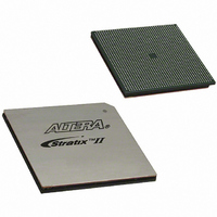
EP2S180F1508C4N Altera, EP2S180F1508C4N Datasheet - Page 155

EP2S180F1508C4N
Manufacturer Part Number
EP2S180F1508C4N
Description
IC STRATIX II FPGA 180K 1508FBGA
Manufacturer
Altera
Series
Stratix® IIr
Datasheet
1.EP2S15F484I4N.pdf
(238 pages)
Specifications of EP2S180F1508C4N
Number Of Logic Elements/cells
179400
Number Of Labs/clbs
8970
Total Ram Bits
9383040
Number Of I /o
1170
Voltage - Supply
1.15 V ~ 1.25 V
Mounting Type
Surface Mount
Operating Temperature
0°C ~ 85°C
Package / Case
1508-FBGA
Family Name
Stratix II
Number Of Logic Blocks/elements
179400
# I/os (max)
1170
Frequency (max)
711.24MHz
Process Technology
90nm (CMOS)
Operating Supply Voltage (typ)
1.2V
Logic Cells
179400
Ram Bits
9383040
Operating Supply Voltage (min)
1.15V
Operating Supply Voltage (max)
1.25V
Operating Temp Range
0C to 85C
Operating Temperature Classification
Commercial
Mounting
Surface Mount
Pin Count
1508
Package Type
FC-FBGA
For Use With
544-1701 - DSP PRO KIT W/SII EP2S180N
Lead Free Status / RoHS Status
Lead free / RoHS Compliant
Number Of Gates
-
Lead Free Status / Rohs Status
Compliant
Other names
544-1887
EP2S180F1508C4N
EP2S180F1508C4N
Available stocks
Company
Part Number
Manufacturer
Quantity
Price
Company:
Part Number:
EP2S180F1508C4N
Manufacturer:
ALTERA
Quantity:
3 000
Part Number:
EP2S180F1508C4N
Manufacturer:
ALTERA/阿尔特拉
Quantity:
20 000
- Current page: 155 of 238
- Download datasheet (3Mb)
Altera Corporation
April 2011
Note to
(1)
25-Ω R
3.3/2.5
50-Ω R
3.3/2.5/1.8
50-Ω R
R
C
C
C
C
C
C
Table 5–31. Series & Differential On-Chip Termination Specification for Left & Right I/O Banks
Table 5–32. Stratix II Device Capacitance
D
I O T B
I O L R
C L K T B
C L K L R
C L K L R +
O U T F B
Symbol
Symbol
Capacitance is sample-tested only. Capacitance is measured using time-domain reflections (TDR). Measurement
accuracy is within ±0.5pF
S
S
S
Table
1.5
5–32:
Input capacitance on I/O pins in I/O banks 3, 4, 7, and 8.
Input capacitance on I/O pins in I/O banks 1, 2, 5, and 6, including high-
speed differential receiver and transmitter pins.
Input capacitance on top/bottom clock input pins:
CLK[12..15]
Input capacitance on left/right clock inputs:
Input capacitance on left/right clock inputs:
CLK11
Input capacitance on dual-purpose clock output/feedback pins in PLL
banks 9, 10, 11, and 12.
Internal differential termination for
LVDS or HyperTransport technology
(100-Ω setting)
Internal series termination without
calibration (25-Ω setting)
Internal series termination without
calibration (50-Ω setting)
Internal series termination without
calibration (50-Ω setting)
.
Description
Pin Capacitance
Table 5–32
.
shows the Stratix II device family pin capacitance.
Parameter
Note (1)
V
V
V
V
C C I O
C C I O
C C I O
C C I O
CLK0
CLK1
Conditions
= 3.3/2.5 V
= 3.3/2.5/1.8 V
= 1.5 V
= 2.5 V
,
,
CLK[4..7]
CLK2
CLK3
,
,
CLK8
CLK9
Stratix II Device Handbook, Volume 1
and
,
, and
DC & Switching Characteristics
Commercial
CLK10
Max
±30
±30
±36
±20
Resistance Tolerance
.
Industrial
Typical
5.0
6.1
6.0
6.1
3.3
6.7
Max
±30
±30
±36
±25
Unit
Unit
%
%
%
%
pF
pF
pF
pF
pF
pF
5–19
Related parts for EP2S180F1508C4N
Image
Part Number
Description
Manufacturer
Datasheet
Request
R

Part Number:
Description:
CYCLONE II STARTER KIT EP2C20N
Manufacturer:
Altera
Datasheet:

Part Number:
Description:
CPLD, EP610 Family, ECMOS Process, 300 Gates, 16 Macro Cells, 16 Reg., 16 User I/Os, 5V Supply, 35 Speed Grade, 24DIP
Manufacturer:
Altera Corporation
Datasheet:

Part Number:
Description:
CPLD, EP610 Family, ECMOS Process, 300 Gates, 16 Macro Cells, 16 Reg., 16 User I/Os, 5V Supply, 15 Speed Grade, 24DIP
Manufacturer:
Altera Corporation
Datasheet:

Part Number:
Description:
Manufacturer:
Altera Corporation
Datasheet:

Part Number:
Description:
CPLD, EP610 Family, ECMOS Process, 300 Gates, 16 Macro Cells, 16 Reg., 16 User I/Os, 5V Supply, 30 Speed Grade, 24DIP
Manufacturer:
Altera Corporation
Datasheet:

Part Number:
Description:
High-performance, low-power erasable programmable logic devices with 8 macrocells, 10ns
Manufacturer:
Altera Corporation
Datasheet:

Part Number:
Description:
High-performance, low-power erasable programmable logic devices with 8 macrocells, 7ns
Manufacturer:
Altera Corporation
Datasheet:

Part Number:
Description:
Classic EPLD
Manufacturer:
Altera Corporation
Datasheet:

Part Number:
Description:
High-performance, low-power erasable programmable logic devices with 8 macrocells, 10ns
Manufacturer:
Altera Corporation
Datasheet:

Part Number:
Description:
Manufacturer:
Altera Corporation
Datasheet:

Part Number:
Description:
Manufacturer:
Altera Corporation
Datasheet:

Part Number:
Description:
Manufacturer:
Altera Corporation
Datasheet:

Part Number:
Description:
CPLD, EP610 Family, ECMOS Process, 300 Gates, 16 Macro Cells, 16 Reg., 16 User I/Os, 5V Supply, 25 Speed Grade, 24DIP
Manufacturer:
Altera Corporation
Datasheet:


