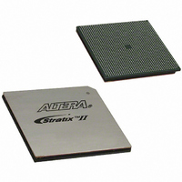
EP2S180F1508C4N Altera, EP2S180F1508C4N Datasheet - Page 132

EP2S180F1508C4N
Manufacturer Part Number
EP2S180F1508C4N
Description
IC STRATIX II FPGA 180K 1508FBGA
Manufacturer
Altera
Series
Stratix® IIr
Datasheet
1.EP2S15F484I4N.pdf
(238 pages)
Specifications of EP2S180F1508C4N
Number Of Logic Elements/cells
179400
Number Of Labs/clbs
8970
Total Ram Bits
9383040
Number Of I /o
1170
Voltage - Supply
1.15 V ~ 1.25 V
Mounting Type
Surface Mount
Operating Temperature
0°C ~ 85°C
Package / Case
1508-FBGA
Family Name
Stratix II
Number Of Logic Blocks/elements
179400
# I/os (max)
1170
Frequency (max)
711.24MHz
Process Technology
90nm (CMOS)
Operating Supply Voltage (typ)
1.2V
Logic Cells
179400
Ram Bits
9383040
Operating Supply Voltage (min)
1.15V
Operating Supply Voltage (max)
1.25V
Operating Temp Range
0C to 85C
Operating Temperature Classification
Commercial
Mounting
Surface Mount
Pin Count
1508
Package Type
FC-FBGA
For Use With
544-1701 - DSP PRO KIT W/SII EP2S180N
Lead Free Status / RoHS Status
Lead free / RoHS Compliant
Number Of Gates
-
Lead Free Status / Rohs Status
Compliant
Other names
544-1887
EP2S180F1508C4N
EP2S180F1508C4N
Available stocks
Company
Part Number
Manufacturer
Quantity
Price
Company:
Part Number:
EP2S180F1508C4N
Manufacturer:
ALTERA
Quantity:
3 000
Part Number:
EP2S180F1508C4N
Manufacturer:
ALTERA/阿尔特拉
Quantity:
20 000
- Current page: 132 of 238
- Download datasheet (3Mb)
Stratix II Hot-Socketing Specifications
4–2
Stratix II Device Handbook, Volume 1
Devices Can Be Driven Before Power-Up
You can drive signals into the I/O pins, dedicated input pins and
dedicated clock pins of Stratix II devices before or during power-up or
power-down without damaging the device. Stratix II devices support any
power-up or power-down sequence (V
to simplify system level design.
I/O Pins Remain Tri-Stated During Power-Up
A device that does not support hot-socketing may interrupt system
operation or cause contention by driving out before or during power-up.
In a hot socketing situation, Stratix II device's output buffers are turned
off during system power-up or power-down. Stratix II device also does
not drive out until the device is configured and has attained proper
operating conditions.
Signal Pins Do Not Drive the V
Supplies
Devices that do not support hot-socketing can short power supplies
together when powered-up through the device signal pins. This irregular
power-up can damage both the driving and driven devices and can
disrupt card power-up.
Stratix II devices do not have a current path from I/O pins, dedicated
input pins, or dedicated clock pins to the V
before or during power-up. A Stratix II device may be inserted into (or
removed from) a powered-up system board without damaging or
interfering with system-board operation. When hot-socketing, Stratix II
devices may have a minimal effect on the signal integrity of the
backplane.
1
■
■
The hot socketing DC specification is: | I
The hot socketing AC specification is: | I
less.
You can power up or power down the V
pins in any sequence. The power supply ramp rates can range
from 100 μs to 100 ms. All V
within 100 ms of each other to prevent I/O pins from driving
out. During hot socketing, the I/O pin capacitance is less than 15
pF and the clock pin capacitance is less than 20 pF. Stratix II
devices meet the following hot socketing specification.
CCIO
CC
, V
CCIO
supplies must power down
CCINT
, V
CCIO
IOPIN
IOPIN
CCINT
or V
, V
CCIO
CCINT
, and V
| < 300 μA.
| < 8 mA for 10 ns or
CCPD
, V
Altera Corporation
, or V
CCINT
Power
CCPD
CCPD
, and V
) in order
May 2007
pins
CCPD
Related parts for EP2S180F1508C4N
Image
Part Number
Description
Manufacturer
Datasheet
Request
R

Part Number:
Description:
CYCLONE II STARTER KIT EP2C20N
Manufacturer:
Altera
Datasheet:

Part Number:
Description:
CPLD, EP610 Family, ECMOS Process, 300 Gates, 16 Macro Cells, 16 Reg., 16 User I/Os, 5V Supply, 35 Speed Grade, 24DIP
Manufacturer:
Altera Corporation
Datasheet:

Part Number:
Description:
CPLD, EP610 Family, ECMOS Process, 300 Gates, 16 Macro Cells, 16 Reg., 16 User I/Os, 5V Supply, 15 Speed Grade, 24DIP
Manufacturer:
Altera Corporation
Datasheet:

Part Number:
Description:
Manufacturer:
Altera Corporation
Datasheet:

Part Number:
Description:
CPLD, EP610 Family, ECMOS Process, 300 Gates, 16 Macro Cells, 16 Reg., 16 User I/Os, 5V Supply, 30 Speed Grade, 24DIP
Manufacturer:
Altera Corporation
Datasheet:

Part Number:
Description:
High-performance, low-power erasable programmable logic devices with 8 macrocells, 10ns
Manufacturer:
Altera Corporation
Datasheet:

Part Number:
Description:
High-performance, low-power erasable programmable logic devices with 8 macrocells, 7ns
Manufacturer:
Altera Corporation
Datasheet:

Part Number:
Description:
Classic EPLD
Manufacturer:
Altera Corporation
Datasheet:

Part Number:
Description:
High-performance, low-power erasable programmable logic devices with 8 macrocells, 10ns
Manufacturer:
Altera Corporation
Datasheet:

Part Number:
Description:
Manufacturer:
Altera Corporation
Datasheet:

Part Number:
Description:
Manufacturer:
Altera Corporation
Datasheet:

Part Number:
Description:
Manufacturer:
Altera Corporation
Datasheet:

Part Number:
Description:
CPLD, EP610 Family, ECMOS Process, 300 Gates, 16 Macro Cells, 16 Reg., 16 User I/Os, 5V Supply, 25 Speed Grade, 24DIP
Manufacturer:
Altera Corporation
Datasheet:


