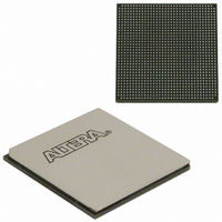
EP1AGX90EF1152I6 Altera, EP1AGX90EF1152I6 Datasheet - Page 137

EP1AGX90EF1152I6
Manufacturer Part Number
EP1AGX90EF1152I6
Description
IC ARRIA GX FPGA 90K 1152FBGA
Manufacturer
Altera
Series
Arria GXr
Datasheet
1.EP1AGX20CF484C6N.pdf
(234 pages)
Specifications of EP1AGX90EF1152I6
Number Of Logic Elements/cells
90220
Number Of Labs/clbs
4511
Total Ram Bits
4477824
Number Of I /o
538
Voltage - Supply
1.15 V ~ 1.25 V
Mounting Type
Surface Mount
Operating Temperature
-40°C ~ 100°C
Package / Case
1152-FBGA
Lead Free Status / RoHS Status
Contains lead / RoHS non-compliant
Number Of Gates
-
Available stocks
Company
Part Number
Manufacturer
Quantity
Price
Company:
Part Number:
EP1AGX90EF1152I6
Manufacturer:
ALTERA
Quantity:
8 831
Company:
Part Number:
EP1AGX90EF1152I6
Manufacturer:
ALTERA
Quantity:
3 000
Chapter 4: DC and Switching Characteristics
Operating Conditions
Table 4–14. Arria GX Device DC Operating Conditions (Part 2 of 2)
I/O Standard Specifications
Table 4–15. LVTTL Specifications
Table 4–16. LVCMOS Specifications
© December 2009 Altera Corporation
R
Notes to
(1) Typical values are for T
(2) This value is specified for normal device operation. The value may vary during power-up. This applies for all V
(3) Maximum values depend on the actual TJ and design utilization. For maximum values, refer to the Excel-based PowerPlay Early Power Estimator
(4) Pin pull-up resistance values will be lower if an external source drives the pin higher than V
V
V
V
V
V
Notes to
(1) Arria GX devices comply to the narrow range for the supply voltage as specified in the EIA/JEDEC Standard, JESD8-B.
(2) This specification is supported across all the programmable drive strength settings available for this I/O standard.
V
V
V
V
V
Notes to
(1) Arria GX devices comply to the narrow range for the supply voltage as specified in the EIA/JEDEC Standard, JESD8-B.
(2) This specification is supported across all the programmable drive strength available for this I/O standard.
CCIO
IH
IL
OH
OL
CCIO
IH
IL
OH
OL
CONF
Symbol
and 1.2 V).
(available at
values. For more information, refer to
Symbol
Symbol
(1)
(1)
(4)
Table
Table
Table
4–14:
4–15:
4–16:
Value of I/O pin pull-up
resistor before and during
configuration
Recommended value of
I/O pin external pull-down
resistor before and during
configuration
PowerPlay Early Power Estimators (EPE) and Power
Output supply voltage
High-level input voltage
Low-level input voltage
High-level output voltage
Low-level output voltage
Output supply voltage
High-level input voltage
Low-level input voltage
High-level output voltage
Low-level output voltage
Parameter
Table 4–15
specifications.
A
= 25 °C, V
Parameter
Parameter
CCINT
through
“Power Consumption” on page
= 1.2 V, and V
V
V
V
V
V
i
i
i
i
i
= 0, V
= 0, V
= 0, V
= 0, V
= 0, V
Table 4–38
I
I
OH
OL
CCIO
= 4 mA
= –4 mA
V
V
Conditions
CCIO
CCIO
CCIO
CCIO
CCIO
CCIO
CCIO
= 1.2 V, 1.5 V, 1.8 V, 2.5 V, and 3.3 V.
Conditions
= 3.3 V
= 2.5 V
= 1.8 V
= 1.5 V
= 1.2 V
—
= 3.0, I
= 3.0, I
(2)
—
—
—
Analyzer) or the Quartus
(2)
show the Arria GX device family I/O standard
Conditions
OH
OL
4–25.
—
—
—
= 0.1 mA
= –0.1 mA
(Note 1)
(2)
Device
(2)
—
—
—
—
—
—
®
Minimum
CCIO
II PowerPlay Power Analyzer feature for maximum
3.135
–0.3
1.7
2.4
—
.
V
Minimum
CCIO
3.135
–0.3
1.7
—
– 0.2
Min
10
15
30
40
50
—
Arria GX Device Handbook, Volume 1
CCIO
Maximum
Typ
25
35
50
75
90
settings (3.3, 2.5, 1.8, 1.5,
1
3.465
Maximum
0.45
4.0
0.8
—
3.465
4.0
0.8
0.2
—
Max
100
150
170
50
70
2
Units
Units
Units
V
V
V
V
V
V
V
V
V
V
k
k
k
k
k
k
4–15


