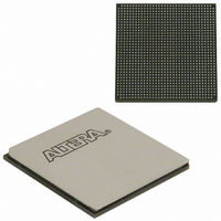
EP1AGX90EF1152I6 Altera, EP1AGX90EF1152I6 Datasheet - Page 100

EP1AGX90EF1152I6
Manufacturer Part Number
EP1AGX90EF1152I6
Description
IC ARRIA GX FPGA 90K 1152FBGA
Manufacturer
Altera
Series
Arria GXr
Datasheet
1.EP1AGX20CF484C6N.pdf
(234 pages)
Specifications of EP1AGX90EF1152I6
Number Of Logic Elements/cells
90220
Number Of Labs/clbs
4511
Total Ram Bits
4477824
Number Of I /o
538
Voltage - Supply
1.15 V ~ 1.25 V
Mounting Type
Surface Mount
Operating Temperature
-40°C ~ 100°C
Package / Case
1152-FBGA
Lead Free Status / RoHS Status
Contains lead / RoHS non-compliant
Number Of Gates
-
Available stocks
Company
Part Number
Manufacturer
Quantity
Price
Company:
Part Number:
EP1AGX90EF1152I6
Manufacturer:
ALTERA
Quantity:
8 831
Company:
Part Number:
EP1AGX90EF1152I6
Manufacturer:
ALTERA
Quantity:
3 000
2–94
Table 2–25. Arria GX Devices Supported I/O Standards
Arria GX Device Handbook, Volume 1
LVTTL
LVCMOS
2.5 V
1.8 V
1.5-V LVCMOS
3.3-V PCI
3.3-V PCI-X mode 1
LVDS
LVPECL
HyperTransport technology
Differential 1.5-V HSTL class I and II
Differential 1.8-V HSTL class I and II
Differential SSTL-18 class I and II
Differential SSTL-2 class I and II
1.2-V HSTL
1.5-V HSTL class I and II
1.8-V HSTL class I and II
SSTL-18 class I and II
SSTL-2 class I and II
Notes to
(1) This I/O standard is only available on input and output column clock pins.
(2) This I/O standard is only available on input clock pins and DQS pins in I/O banks 3, 4, 7, and 8, and output clock pins in I/O banks 9, 10, 11,
(3) V
(4) 1.2-V HSTL is only supported in I/O banks 4, 7, and 8.
and 12.
CCIO
Table
is 3.3 V when using this I/O standard in input and output column clock pins (in I/O banks 3, 4, 7, 8, 9, 10, 11, and 12).
(1)
(4)
f
2–25:
I/O Standard
Table 2–25
For more information about the I/O standards supported by Arria GX I/O banks,
refer to the
Arria GX devices contain six I/O banks and four enhanced PLL external clock output
banks, as shown in
circuitry to support source-synchronous, high-speed differential I/O for LVDS inputs
and outputs. These banks support all Arria GX I/O standards except PCI or PCI-X
I/O pins, and SSTL-18 class II and HSTL outputs. The top and bottom I/O banks
support all single-ended I/O standards. Additionally, enhanced PLL external clock
output banks allow clock output capabilities such as differential support for SSTL and
HSTL.
(2)
(2)
describes the I/O standards supported by Arria GX devices.
Selectable I/O Standards in Arria GX Devices
(2)
(2)
Single-ended
Single-ended
Single-ended
Single-ended
Single-ended
Single-ended
Single-ended
Differential
Differential
Differential
Differential
Differential
Differential
Differential
Voltage-referenced
Voltage-referenced
Voltage-referenced
Voltage-referenced
Voltage-referenced
Figure
Type
2–78. The two I/O banks on the left of the device contain
Input Reference
Voltage
(V
0.75
0.90
0.90
1.25
0.75
0.90
1.25
REF
0.6
0.9
—
—
—
—
—
—
—
—
—
—
) (V)
chapter.
Output Supply
(V
© December 2009 Altera Corporation
Voltage
2.5
2.5
CCIO
3.3
3.3
2.5
1.8
1.5
3.3
3.3
3.3
1.5
1.8
1.8
2.5
1.2
1.5
1.8
1.8
2.5
Chapter 2: Arria GX Architecture
(3)
(3)
) (V)
Voltage (V
Termination
Board
0.75
0.90
0.90
1.25
0.75
0.90
1.25
0.6
0.9
—
—
—
—
—
—
—
—
—
—
I/O Structure
TT
) (V)


