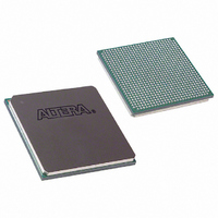
EP3C120F780C8N Altera, EP3C120F780C8N Datasheet - Page 152

EP3C120F780C8N
Manufacturer Part Number
EP3C120F780C8N
Description
IC CYCLONE III FPGA 119K 780FBGA
Manufacturer
Altera
Series
Cyclone® IIIr
Datasheets
1.EP3C5F256C8N.pdf
(5 pages)
2.EP3C5F256C8N.pdf
(34 pages)
3.EP3C5F256C8N.pdf
(66 pages)
4.EP3C5F256C8N.pdf
(14 pages)
5.EP3C5F256C8N.pdf
(76 pages)
6.EP3C120F780C8N.pdf
(274 pages)
Specifications of EP3C120F780C8N
Number Of Logic Elements/cells
119088
Number Of Labs/clbs
7443
Total Ram Bits
3981312
Number Of I /o
531
Voltage - Supply
1.15 V ~ 1.25 V
Mounting Type
Surface Mount
Operating Temperature
0°C ~ 85°C
Package / Case
780-FBGA
Family Name
Cyclone III
Number Of Logic Blocks/elements
119088
# I/os (max)
531
Frequency (max)
402MHz
Process Technology
65nm
Operating Supply Voltage (typ)
1.2V
Logic Cells
119088
Ram Bits
3981312
Operating Supply Voltage (min)
1.15V
Operating Supply Voltage (max)
1.25V
Operating Temp Range
0C to 85C
Operating Temperature Classification
Commercial
Mounting
Surface Mount
Pin Count
780
Package Type
FBGA
For Use With
544-2601 - KIT DEV CYCLONE III LS EP3CLS200544-2589 - KIT DEV EMB CYCLONE III EDITION544-2566 - KIT DEV DSP CYCLONE III EDITION544-2444 - KIT DEV CYCLONE III EP3C120544-2411 - KIT DEV NIOS II CYCLONE III ED.
Lead Free Status / RoHS Status
Lead free / RoHS Compliant
Number Of Gates
-
Lead Free Status / Rohs Status
Compliant
Other names
544-2392
544-2533
544-2533
EP3C120F780C8NES
544-2533
544-2533
EP3C120F780C8NES
Available stocks
Company
Part Number
Manufacturer
Quantity
Price
Company:
Part Number:
EP3C120F780C8N
Manufacturer:
ALTERA
Quantity:
642
Part Number:
EP3C120F780C8N
Manufacturer:
ALTERA/阿尔特拉
Quantity:
20 000
8–8
Figure 8–2. DQS, CQ, or CQ# Pins in Cyclone III Device Family I/O Banks
Note to
(1) The DQS, CQ, or CQ# pin locations in this diagram apply to all packages in Cyclone III device family except devices in 144-pin EQFP and 164-pin
Cyclone III Device Handbook, Volume 1
MBGA.
Figure
8–2:
1
1
Each DQ group is associated with its corresponding DQS pins, as defined in the
Cyclone III and Cyclone III LS pin tables; for example:
The Quartus
with its associated DQS.
Figure 8–2
Cyclone III device family I/O banks.
For Cyclone III device family memory interface support, only one interface is placed
on each side.
■
■
DQS1L/CQ1L#
DQS3L/CQ3L#
For DDR2 or DDR SDRAM, ×8 DQ group DQ3B[7:0] pins are associated with
the DQS3B pin (same 3B group index)
For QDR II SRAM, ×9 Q read-data group DQ3L[8..0] pins are associated
with DQS2L/CQ3L and DQS3L/CQ3L# pins (same 3L group index)
DQS2L/CQ3L
DQS0L/CQ1L
shows the location and numbering of the DQS, DQ, or CQ# pins in the
®
II software issues an error message if a DQ group is not placed properly
I/O Bank 3
I/O Bank 8
Cyclone III Device Family
Chapter 8: External Memory Interfaces in the Cyclone III Device Family
I/O Bank 7
I/O Bank 4
(Note 1)
Cyclone III Device Family Memory Interfaces Pin Support
DQS3R/CQ3R#
DQS0R/CQ1R
DQS1R/CQ1R#
DQS2R/CQ3R
© January 2010 Altera Corporation


