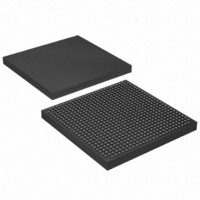
EP1S10F672C7 Altera, EP1S10F672C7 Datasheet - Page 65

EP1S10F672C7
Manufacturer Part Number
EP1S10F672C7
Description
IC STRATIX FPGA 10K LE 672-FBGA
Manufacturer
Altera
Series
Stratix®r
Datasheet
1.EP1S10F780C7.pdf
(276 pages)
Specifications of EP1S10F672C7
Number Of Logic Elements/cells
10570
Number Of Labs/clbs
1057
Total Ram Bits
920448
Number Of I /o
345
Voltage - Supply
1.425 V ~ 1.575 V
Mounting Type
Surface Mount
Operating Temperature
0°C ~ 85°C
Package / Case
672-FBGA
Family Name
Stratix
Number Of Logic Blocks/elements
10570
# I/os (max)
345
Frequency (max)
420.17MHz
Process Technology
0.13um (CMOS)
Operating Supply Voltage (typ)
1.5V
Logic Cells
10570
Ram Bits
920448
Operating Supply Voltage (min)
1.425V
Operating Supply Voltage (max)
1.575V
Operating Temp Range
0C to 85C
Operating Temperature Classification
Commercial
Mounting
Surface Mount
Pin Count
672
Package Type
FBGA
Lead Free Status / RoHS Status
Contains lead / RoHS non-compliant
Number Of Gates
-
Lead Free Status / Rohs Status
Not Compliant
Other names
544-1109
Available stocks
Company
Part Number
Manufacturer
Quantity
Price
Company:
Part Number:
EP1S10F672C7
Manufacturer:
ALTERA
Quantity:
3 000
Part Number:
EP1S10F672C7
Manufacturer:
XILINX/赛灵思
Quantity:
20 000
Company:
Part Number:
EP1S10F672C7AA
Manufacturer:
ALTERA
Quantity:
3 000
Company:
Part Number:
EP1S10F672C7ES
Manufacturer:
ALTERA
Quantity:
89
Company:
Part Number:
EP1S10F672C7N
Manufacturer:
ALTERA
Quantity:
3 000
Part Number:
EP1S10F672C7N
Manufacturer:
ALTERA/阿尔特拉
Quantity:
20 000
Figure 2–28. Single-Port Mode
Note to
(1)
Altera Corporation
July 2005
address[ ]
outclken
outclock
inclken
inclock
data[ ]
wren
Violating the setup or hold time on the address registers could corrupt the memory contents. This applies to both
read and write operations.
Figure
8 LAB Row
Clocks
8
2–28:
Single-Port Mode
The memory blocks also support single-port mode, used when
simultaneous reads and writes are not required. See
block in a memory block can support up to two single-port mode RAM
blocks in the M4K RAM blocks if each RAM block is less than or equal to
2K bits in size.
Note (1)
D
ENA
D
ENA
Q
Q
Generator
D
ENA
Pulse
Write
Q
Data In
Address
Write Enable
RAM/ROM
1,024 × 4
2,048 × 2
4,096 × 1
Data Out
256 × 16
512 × 8
Stratix Device Handbook, Volume 1
D
ENA
Q
Figure
Stratix Architecture
2–28. A single
To MultiTrack
Interconnect
2–51


