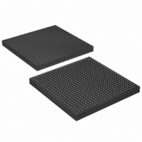
EP1S10F672C7 Altera, EP1S10F672C7 Datasheet - Page 118

EP1S10F672C7
Manufacturer Part Number
EP1S10F672C7
Description
IC STRATIX FPGA 10K LE 672-FBGA
Manufacturer
Altera
Series
Stratix®r
Datasheet
1.EP1S10F780C7.pdf
(276 pages)
Specifications of EP1S10F672C7
Number Of Logic Elements/cells
10570
Number Of Labs/clbs
1057
Total Ram Bits
920448
Number Of I /o
345
Voltage - Supply
1.425 V ~ 1.575 V
Mounting Type
Surface Mount
Operating Temperature
0°C ~ 85°C
Package / Case
672-FBGA
Family Name
Stratix
Number Of Logic Blocks/elements
10570
# I/os (max)
345
Frequency (max)
420.17MHz
Process Technology
0.13um (CMOS)
Operating Supply Voltage (typ)
1.5V
Logic Cells
10570
Ram Bits
920448
Operating Supply Voltage (min)
1.425V
Operating Supply Voltage (max)
1.575V
Operating Temp Range
0C to 85C
Operating Temperature Classification
Commercial
Mounting
Surface Mount
Pin Count
672
Package Type
FBGA
Lead Free Status / RoHS Status
Contains lead / RoHS non-compliant
Number Of Gates
-
Lead Free Status / Rohs Status
Not Compliant
Other names
544-1109
Available stocks
Company
Part Number
Manufacturer
Quantity
Price
Company:
Part Number:
EP1S10F672C7
Manufacturer:
ALTERA
Quantity:
3 000
Part Number:
EP1S10F672C7
Manufacturer:
XILINX/赛灵思
Quantity:
20 000
Company:
Part Number:
EP1S10F672C7AA
Manufacturer:
ALTERA
Quantity:
3 000
Company:
Part Number:
EP1S10F672C7ES
Manufacturer:
ALTERA
Quantity:
89
Company:
Part Number:
EP1S10F672C7N
Manufacturer:
ALTERA
Quantity:
3 000
Part Number:
EP1S10F672C7N
Manufacturer:
ALTERA/阿尔特拉
Quantity:
20 000
I/O Structure
I/O Structure
2–104
Stratix Device Handbook, Volume 1
Control Signals
The fast PLL has the same lock output, pllenable input, and areset
input control signals as the enhanced PLL.
If the input clock stops and causes the PLL to lose lock, then the PLL must
be reset for correct phase shift operation.
For more information on high-speed differential I/O support, see
Speed Differential I/O Support” on page
IOEs provide many features, including:
■
■
■
■
■
■
■
■
■
■
■
■
■
■
■
The IOE in Stratix devices contains a bidirectional I/O buffer, six
registers, and a latch for a complete embedded bidirectional single data
rate or DDR transfer.
IOE contains two input registers (plus a latch), two output registers, and
two output enable registers. The design can use both input registers and
the latch to capture DDR input and both output registers to drive DDR
outputs. Additionally, the design can use the output enable (OE) register
for fast clock-to-output enable timing. The negative edge-clocked OE
register is used for DDR SDRAM interfacing. The Quartus II software
automatically duplicates a single OE register that controls multiple
output or bidirectional pins.
Dedicated differential and single-ended I/O buffers
3.3-V, 64-bit, 66-MHz PCI compliance
3.3-V, 64-bit, 133-MHz PCI-X 1.0 compliance
Joint Test Action Group (JTAG) boundary-scan test (BST) support
Differential on-chip termination for LVDS I/O standard
Programmable pull-up during configuration
Output drive strength control
Slew-rate control
Tri-state buffers
Bus-hold circuitry
Programmable pull-up resistors
Programmable input and output delays
Open-drain outputs
DQ and DQS I/O pins
Double-data rate (DDR) Registers
Figure 2–59
shows the Stratix IOE structure. The
2–130.
Altera Corporation
July 2005
“High-


