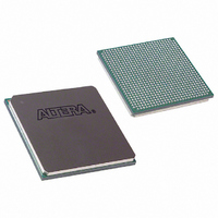
EP3C40F780I7 Altera, EP3C40F780I7 Datasheet - Page 101

EP3C40F780I7
Manufacturer Part Number
EP3C40F780I7
Description
IC CYCLONE III FPGA 40K 780 FBGA
Manufacturer
Altera
Series
Cyclone® IIIr
Datasheets
1.EP3C5F256C8N.pdf
(5 pages)
2.EP3C5F256C8N.pdf
(34 pages)
3.EP3C5F256C8N.pdf
(66 pages)
4.EP3C5F256C8N.pdf
(14 pages)
5.EP3C5F256C8N.pdf
(76 pages)
6.EP3C40F780I7.pdf
(274 pages)
Specifications of EP3C40F780I7
Number Of Logic Elements/cells
39600
Number Of Labs/clbs
2475
Total Ram Bits
1161216
Number Of I /o
535
Voltage - Supply
1.15 V ~ 1.25 V
Mounting Type
Surface Mount
Operating Temperature
-40°C ~ 100°C
Package / Case
780-FBGA
Family Name
Cyclone III
Number Of Logic Blocks/elements
39600
# I/os (max)
535
Frequency (max)
437.5MHz
Process Technology
65nm
Operating Supply Voltage (typ)
1.2V
Logic Cells
39600
Ram Bits
1161216
Operating Supply Voltage (min)
1.15V
Operating Supply Voltage (max)
1.25V
Operating Temp Range
-40C to 100C
Operating Temperature Classification
Industrial
Mounting
Surface Mount
Pin Count
780
Package Type
FBGA
Lead Free Status / RoHS Status
Contains lead / RoHS non-compliant
Number Of Gates
-
Lead Free Status / Rohs Status
Not Compliant
Available stocks
Company
Part Number
Manufacturer
Quantity
Price
Company:
Part Number:
EP3C40F780I7N
Manufacturer:
MINGTEK
Quantity:
2 300
Company:
Part Number:
EP3C40F780I7N
Manufacturer:
ALTERA20
Quantity:
576
Part Number:
EP3C40F780I7N
Manufacturer:
ALTERA/阿尔特拉
Quantity:
20 000
Cyclone III Device Family I/O Elements
© December 2009
CIII51007-3.2
Altera Corporation
This chapter describes the I/O features offered in the Cyclone
(Cyclone III and Cyclone III LS devices).
The I/O capabilities of the Cyclone III device family are driven by the diversification
of I/O standards in many low-cost applications, and the significant increase in
required I/O performance. Altera’s objective is to create a device that accommodates
your key board design needs with ease and flexibility.
The I/O flexibility of the Cyclone III device family is increased from the previous
generation low-cost FPGAs by allowing all I/O standards to be selected on all I/O
banks. Improvements to on-chip termination (OCT) support and the addition of true
differential buffers have eliminated the need for external resistors in many
applications, such as display system interfaces. Altera’s Quartus
completes the solution with powerful pin planning features that allow you to plan
and optimize I/O system designs even before the design files are available.
This chapter contains the following sections:
■
■
■
■
■
■
■
Cyclone III device family I/O elements (IOEs) contain a bidirectional I/O buffer and
five registers for registering input, output, output-enable signals, and complete
embedded bidirectional single-data rate transfer. I/O pins support various
single-ended and differential I/O standards.
The IOE contains one input register, two output registers, and two output-enable
(OE) registers. The two output registers and two OE registers are used for DDR
applications. You can use input registers for fast setup times and output registers for
fast clock-to-output times. Additionally, you can use OE registers for fast
clock-to-output enable timing. You can use IOEs for input, output, or bidirectional
data paths.
“Cyclone III Device Family I/O Elements” on page 6–1
“I/O Element Features” on page 6–2
“OCT Support” on page 6–7
“I/O Standards” on page 6–11
“Termination Scheme for I/O Standards” on page 6–13
“I/O Banks” on page 6–16
“Pad Placement and DC Guidelines” on page 6–21
6. I/O Features in the Cyclone III
Cyclone III Device Handbook, Volume 1
®
III device family
Device Family
®
II software


